TEM vs SEM for Catalyst Analysis: Choosing the Right Electron Microscopy for Your Research
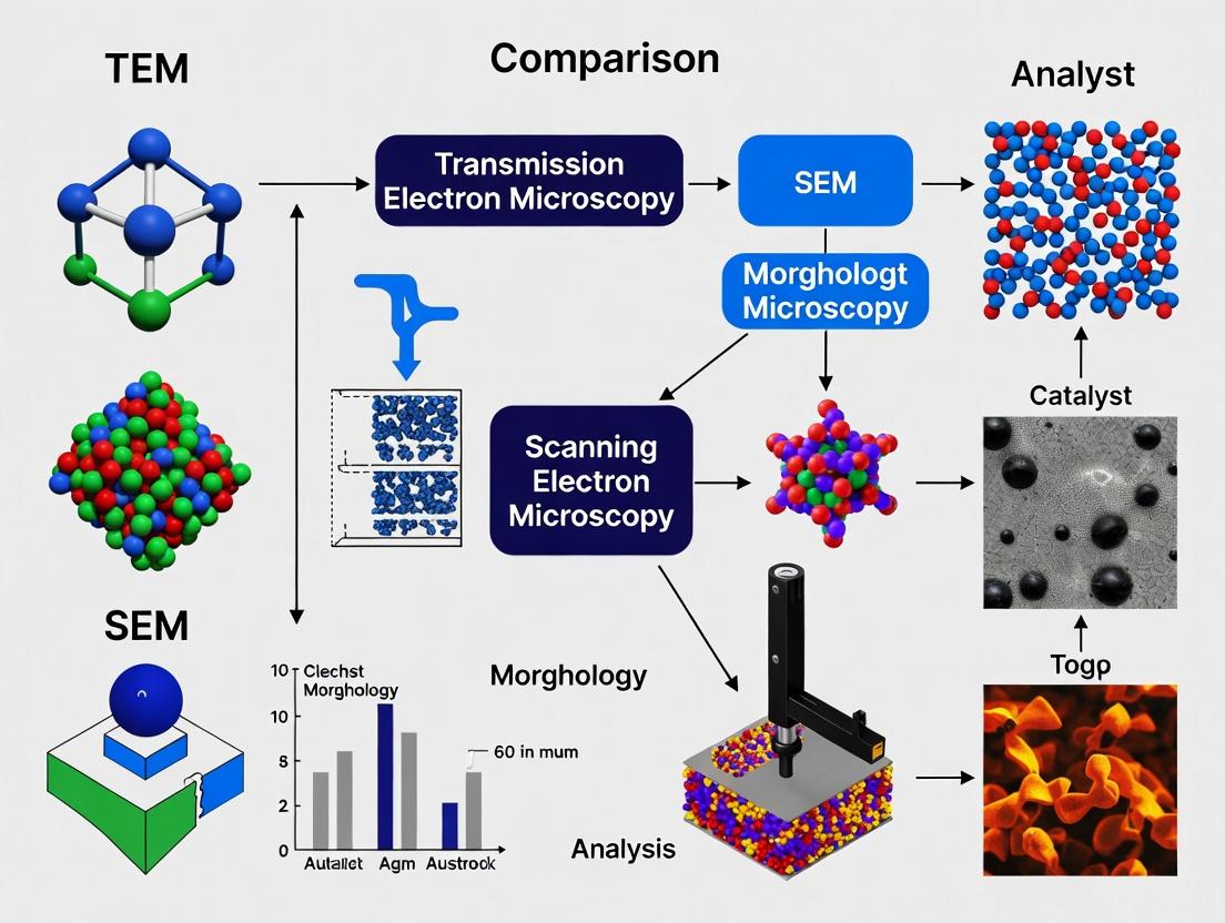
This article provides a comprehensive guide for researchers and drug development professionals on selecting and applying Transmission (TEM) and Scanning (SEM) Electron Microscopy for catalyst morphology analysis.
TEM vs SEM for Catalyst Analysis: Choosing the Right Electron Microscopy for Your Research
Abstract
This article provides a comprehensive guide for researchers and drug development professionals on selecting and applying Transmission (TEM) and Scanning (SEM) Electron Microscopy for catalyst morphology analysis. It covers the fundamental principles of each technique, detailed methodologies for sample preparation and imaging, common troubleshooting scenarios, and a direct comparison of their capabilities for validation. The guide synthesizes current best practices to help scientists optimize their characterization strategy for nanomaterials crucial to catalysis, including those with biomedical applications.
Understanding the Core Principles: How TEM and SEM Work for Catalyst Imaging
This comparison guide is framed within a broader thesis on selecting between Transmission Electron Microscopy (TEM) and Scanning Electron Microscopy (SEM) for catalyst morphology analysis, a critical area for researchers in catalysis and materials science for drug development.
Core Physical Interactions and Data Comparison
The fundamental difference lies in the nature of the electron-beam interaction with the specimen. TEM relies on the transmission of a high-energy electron beam through an ultrathin sample, while SEM images the sample surface by detecting signals from the interaction of a focused beam with a bulk sample.
Table 1: Fundamental Comparison of Electron-Beam Interactions
| Parameter | Transmission Electron Microscope (TEM) | Scanning Electron Microscope (SEM) |
|---|---|---|
| Primary Beam Energy | Typically 60-300 keV | Typically 0.1-30 keV |
| Sample Thickness | Ultrathin (<150 nm) | Bulk (mm scale) |
| Primary Signal Detected | Transmitted/Scattered Electrons | Secondary Electrons (SE), Backscattered Electrons (BSE) |
| Interaction Volume | Confined to thin sample thickness | Pear-shaped, from nm to µm into surface |
| Spatial Resolution | <0.05 nm (atomic resolution) | 0.5-3 nm (surface topography) |
| Primary Information | Internal structure, crystallography, phase composition | Surface topography, composition (via BSE/EDS) |
| Typical Magnification | 50x - 10,000,000x | 10x - 500,000x |
Table 2: Suitability for Catalyst Morphology Analysis
| Analysis Goal | Recommended Instrument | Key Experimental Reason |
|---|---|---|
| Nanoparticle Size Distribution (bulk) | SEM | Faster, larger field of view for statistical analysis. |
| Atomic Structure of Single Nanoparticle | TEM | Lattice imaging and atomic column resolution. |
| Surface Porosity & 3D Topography | SEM | Superior depth of field and 3D reconstruction. |
| Core-Shell Particle Internal Interface | TEM (STEM-HAADF) | Z-contrast imaging reveals internal composition gradients. |
| Elemental Mapping of Agglomerates | SEM-EDS | Efficient for micron-scale areas; quantifiable bulk composition. |
| Oxidation State & Fine Structure | TEM (EELS) | High-energy resolution spectroscopy on nanometric areas. |
Experimental Protocols for Catalyst Characterization
Protocol 1: TEM Analysis of Catalyst Nanoparticles
- Sample Preparation: Disperse catalyst powder in ethanol via ultrasonication for 10 minutes. Drop-cast onto a lacey carbon-coated copper TEM grid. Dry under an IR lamp.
- Instrument Setup: Insert grid into holder. Load into TEM column. Achieve high vacuum (<10^-5 Pa). Align microscope (gun tilt, condenser stigmator). Select acceleration voltage (e.g., 200 keV).
- Imaging: Locate a suitably thin area at low magnification. Switch to high magnification (e.g., 600kX). Adjust objective lens focus and stigmator for optimal phase contrast (for HRTEM) or use STEM mode with HAADF detector.
- Data Acquisition: Acquire images and diffraction patterns. For analysis, use software (e.g., ImageJ) to measure particle size distribution from multiple images (>200 particles).
Protocol 2: SEM Analysis of Catalyst Morphology
- Sample Preparation: Mount catalyst powder on an aluminum stub using conductive carbon tape. Sputter-coat with a 5-10 nm layer of Pt/Pd to ensure conductivity for non-metallic catalysts.
- Instrument Setup: Insert stub into chamber. Pump to high vacuum (~10^-3 to 10^-4 Pa). Turn on electron gun (set voltage, e.g., 5-15 keV). Align aperture.
- Imaging: Navigate to area of interest at low magnification using the secondary electron (SE) detector for topography. Optimize working distance (e.g., 10 mm), focus, and stigmation. Switch to BSE detector for compositional contrast.
- Data Acquisition: Acquire micrographs at various magnifications. For EDS elemental mapping, define a region of interest, set live time (e.g., 100 s), and acquire spectrum.
Visualizing the Workflows
Title: TEM Workflow for Catalyst Analysis
Title: SEM Workflow for Catalyst Analysis
Title: Beam Interaction Volume: TEM vs. SEM
The Scientist's Toolkit: Research Reagent Solutions
Table 3: Essential Materials for EM Catalyst Sample Preparation
| Item | Function in Catalyst Analysis |
|---|---|
| Lacey Carbon TEM Grids | Provides an ultrathin, low-background support film with holes, ideal for imaging unsupported catalyst nanoparticles at high resolution. |
| High-Purity Ethanol/Isopropanol | Solvent for dispersing catalyst powders via ultrasonication to break soft agglomerates before drop-casting. |
| Conductive Carbon Tape | Used to mount powder samples on SEM stubs, providing both adhesion and electrical conductivity to prevent charging. |
| Pt/Pd Sputter Coater | Deposits a nanoscale conductive metal layer on non-conductive catalysts to eliminate charging artifacts in SEM imaging. |
| Ultramicrotome with Diamond Knife | For preparing thin cross-sectional slices of catalyst pellets or embedded powders for TEM, revealing internal porosity. |
| Focused Ion Beam (FIB) System | Enables site-specific extraction of electron-transparent lamellae from precise locations in a bulk catalyst for TEM analysis. |
| EDS Calibration Standard | A known standard (e.g., Cu, Co) required for quantitative energy-dispersive X-ray spectroscopy elemental analysis in both SEM and TEM. |
| Holey Amorphous Carbon Film | An alternative TEM support film that provides a more uniform substrate for quantitative particle size/distribution analysis. |
Within the thesis context of catalyst morphology analysis via electron microscopy, the fundamental distinction between transmission (TEM) and emission (SEM) signal generation dictates analytical capability. TEM analyzes electrons transmitted through an ultrathin sample, revealing internal structure. SEM analyzes electrons emitted from the sample surface (secondary electrons) or backscattered from near-surface regions, revealing topographical and compositional data.
Performance Comparison & Experimental Data
The following table summarizes core performance distinctions based on current experimental data relevant to catalyst research.
| Analytical Feature | Transmission Electron Microscopy (TEM) | Scanning Electron Microscopy (SEM) |
|---|---|---|
| Primary Signal | Electrons transmitted through the sample. | Electrons emitted from the sample surface (SE, BSE). |
| Resolution (Typical) | < 0.1 nm (HRTEM). | 0.5 nm to 3 nm (for secondary electrons). |
| Primary Information | Internal crystal structure, lattice fringes, atomic arrangement, crystallographic phase. | Surface topography, particle size/distribution, elemental composition (with EDS). |
| Sample Thickness Requirement | Ultrathin (< 100 nm). Electrons must penetrate. | Bulk samples. No penetration required. |
| Typical Catalyst Application | Atomic-scale imaging of nanoparticle facets, core-shell structures, and defects. | 3D aggregate morphology, pore structure, and mapping of elemental distribution over large areas. |
| Quantitative Data Example | Lattice spacing measurement: e.g., Pt (111) planes imaged at 0.226 nm. | Particle size distribution: e.g., 5.2 nm ± 1.3 nm average diameter from 500 particles. |
Experimental Protocols
Protocol 1: TEM Analysis of Pt Catalyst Nanoparticles
- Sample Preparation: Dispersed catalyst powder in ethanol via ultrasonication for 10 min. A drop of suspension was deposited on a lacy carbon TEM grid and dried.
- Imaging: Grid loaded into TEM (e.g., JEOL JEM-F200) operating at 200 kV.
- Alignment: Instrument aligned for high-resolution (HRTEM) mode. Astigmatism corrected.
- Data Acquisition: Micrographs taken at various magnifications (50kX to 1.5M X). Fast Fourier Transform (FFT) performed on HRTEM images to confirm crystallinity and measure lattice spacings.
Protocol 2: SEM Analysis of Catalyst Pellet Morphology
- Sample Preparation: Catalyst pellet mounted on aluminum stub with conductive carbon tape. Sputter-coated with 5 nm of Pt/Pd to enhance conductivity.
- Imaging: Sample loaded into FEG-SEM (e.g., Thermo Scientific Apreo 2) operating at 5 kV for high-resolution topography or 15 kV with backscattered electron (BSE) detector for compositional contrast.
- Data Acquisition: Secondary electron (SE) images acquired at various magnifications to assess surface texture. Energy-dispersive X-ray spectroscopy (EDS) maps collected at 15 kV to correlate morphology with elemental distribution.
Diagrams
Signal Generation in TEM vs. SEM
Catalyst Analysis Workflow
The Scientist's Toolkit: Research Reagent Solutions
| Item | Function in Catalyst EM Analysis |
|---|---|
| Lacy Carbon TEM Grids | Support film for ultrathin samples; minimal background interference for high-resolution TEM. |
| Conductive Carbon Tape | Mounts non-conductive samples to SEM stub, preventing charging artifacts. |
| Pt/Pd Sputter Coater | Applies ultra-thin conductive metal layer to insulating samples for SEM, minimizing beam damage. |
| High-Purity Ethanol | Dispersant for creating uniform suspensions of catalyst powders for TEM grid preparation. |
| Ultrasonic Bath | Ensures de-agglomeration of catalyst nanoparticles in suspension prior to TEM sampling. |
| EDS Calibration Standard | (e.g., Cu grid) Verifies accuracy of energy-dispersive X-ray spectroscopy for elemental analysis in both SEM and TEM. |
| Focused Ion Beam (FIB) System | (Advanced) Prepares site-specific, electron-transparent lamellae from bulk catalysts for cross-sectional TEM analysis. |
Within a research thesis focused on catalyst morphology analysis, selecting between Transmission Electron Microscopy (TEM) and Scanning Electron Microscopy (SEM) hinges on a fundamental understanding of their distinct instrument architectures. While both utilize electron beams to probe nanoscale features, their design principles, operational modes, and resultant data types differ substantially. This guide provides an objective, data-driven comparison of TEM and SEM architectures, detailing their implications for catalyst research.
Core Architectural Comparison
The primary architectural difference lies in the beam-sample-detector relationship. SEM employs a finely focused electron beam scanned across the specimen surface, collecting emitted or backscattered electrons. TEM transmits a broad, stationary beam through an ultra-thin specimen, capturing the transmitted electrons. This fundamental distinction dictates all subsequent design choices.
Table 1: Core Instrument Architecture & Specifications
| Component | Transmission Electron Microscope (TEM) | Scanning Electron Microscope (SEM) |
|---|---|---|
| Electron Source | High-brightness field emission gun (FEG) typical. | Tungsten filament, Cerium Hexaboride (CeB6), or FEG. |
| Accelerating Voltage | High (80-300 kV typical for HRTEM). | Lower (0.1-30 kV typical for surface imaging). |
| Beam-Sample Interaction | Stationary, broad beam transmits through thin sample (<150 nm). | Focused, scanning raster across sample surface. |
| Primary Detectors | Fluorescent screen, CCD/CMOS camera, STEM detectors. | Everhart-Thornley SE detector, In-lens SE detector, Backscattered Electron (BSE) detector. |
| Key Sample Requirement | Electron-transparent (ultra-thin films, nanoparticles). | Solid, conductive (or coated) bulk samples. |
| Vacuum Requirement | Ultra-high vacuum (~10⁻⁷ Pa or better) for high-resolution. | High vacuum (~10⁻³ to 10⁻⁵ Pa) typical. |
| Primary Data Output | 2D projection image, diffraction pattern. | 3D-like surface topography image, elemental maps (with EDS). |
Table 2: Performance in Catalyst Morphology Analysis
| Analysis Parameter | TEM Advantage/Application | SEM Advantage/Application |
|---|---|---|
| Resolution | Atomic-scale (≤0.1 nm) lattice imaging. | Nanoscale (0.5-3 nm) surface feature imaging. |
| Morphology Depth | Internal structure, crystallographic defects, grain boundaries. | Surface topography, particle size/distribution, porosity. |
| Statistical Relevance | Limited field of view; high detail on few particles. | Large field of view; better statistics on particle populations. |
| Elemental Analysis | High spatial resolution EELS/EDS, but small analysis volume. | Standard EDS mapping of larger surface areas. |
| Sample Preparation | Complex (ultramicrotomy, ion milling, dispersion). | Simpler (mounting, sputter coating for non-conductors). |
Experimental Protocols for Catalyst Analysis
Protocol 1: TEM Analysis of Nanoparticle Catalysts (Size & Lattice Structure)
- Sample Prep: Ultrasonicate catalyst powder in ethanol. Drop-cast suspension onto a lacey carbon TEM grid. Dry in a desiccator.
- Instrument Setup: Insert grid into a FEG-TEM holder. Align microscope at 200 kV. Establish standard bright-field imaging conditions.
- Imaging: Locate a suitable, thin area. Acquire low-magnification images for particle size distribution. Switch to high-resolution mode (HRTEM) on isolated particles. Adjust defocus to achieve contrast.
- Data Acquisition: Capture HRTEM images and Selected Area Electron Diffraction (SAED) patterns using a direct electron detector.
- Analysis: Use digital image analysis software (e.g., ImageJ) to measure particle diameters. Index SAED rings to identify crystal phases. Analyze lattice fringes in HRTEM images.
Protocol 2: SEM Analysis of Catalyst Pellet Morphology & Composition
- Sample Prep: Mount a catalyst pellet or powder on an aluminum stub using conductive carbon tape. Sputter-coat with a thin (~5 nm) layer of gold or iridium if non-conductive.
- Instrument Setup: Insert stub into chamber of a FEG-SEM. Pump to high vacuum. Set accelerating voltage to 5-15 kV to optimize surface detail.
- Imaging: Use the in-lens SE detector for high-resolution surface topography. Use the BSE detector for atomic number contrast (identifying heavy/light elements).
- EDS Mapping: At a defined region of interest, activate the Energy Dispersive X-ray Spectrometer (EDS). Acquire spectral maps for relevant elements (e.g., Pt, Co, O).
- Analysis: Use built-in software to measure pore sizes and particle agglomerates. Overlay EDS maps to correlate elemental distribution with surface features.
The Scientist's Toolkit: Key Research Reagent Solutions
| Item | Function in TEM/SEM Sample Preparation |
|---|---|
| Lacey Carbon TEM Grids | Provides an ultra-thin, fenestrated support film for nanoparticles, minimizing background noise. |
| Conductive Carbon Tape | Adheres bulk or powder SEM samples to stubs, providing a path to ground to prevent charging. |
| Iridium Sputter Coater | Applies an ultra-fine, conductive metal coating to non-conductive SEM samples, superior for high-resolution. |
| Ultramicrotome & Diamond Knife | Slices bulk catalyst-embedded resin into electron-transparent thin sections (<100 nm) for cross-sectional TEM. |
| Ion Milling System (e.g., PIPS) | Uses argon ions to precisely thin specific sites of a TEM sample to electron transparency, ideal for focused site analysis. |
| High-Purity Ethanol (Absolute) | Suspension medium for dispersing catalyst powders onto TEM grids without leaving residue. |
Architectural & Analytical Workflow Diagrams
Diagram 1: Comparative electron-optical pathways of TEM and SEM.
Diagram 2: Decision logic for selecting TEM or SEM in catalyst research.
In catalyst morphology analysis, selecting the appropriate electron microscopy technique is paramount to elucidating structure-property relationships. This guide frames the comparison between Transmission Electron Microscopy (TEM) and Scanning Electron Microscopy (SEM) within a broader thesis on catalyst characterization. The core distinction lies in their primary information output: TEM provides detailed internal structure and crystallographic data, while SEM offers comprehensive three-dimensional surface topography. The choice directly impacts the interpretation of catalyst morphology, pore structure, nanoparticle dispersion, and active site distribution.
Core Comparison of Primary Outputs
The fundamental difference in operation leads to divergent data types, as summarized in the table below.
Table 1: Core Comparison of TEM and SEM for Catalyst Analysis
| Feature | Transmission Electron Microscopy (TEM) | Scanning Electron Microscopy (SEM) |
|---|---|---|
| Primary Beam | High-energy (60-300 kV) electrons transmitted through a thin specimen. | Focused beam of lower-energy (0.1-30 kV) electrons scanned across the surface. |
| Primary Information | Internal Structure: Projected 2D image of sample interior, atomic-scale lattice fringes, crystallographic phase (via diffraction). | Surface Topography: 3D-like image of surface features, texture, and morphology. |
| Resolution | Sub-nanometer to atomic-scale (≤ 0.1 nm for HRTEM). | ~0.5 nm to 5 nm (dependent on beam energy and signal). |
| Sample Requirements | Ultra-thin (< 100 nm). Requires extensive preparation (ultramicrotomy, ion milling, FIB lift-out). | Bulk or thick samples. Minimal preparation; requires conductive coating for non-conductive catalysts. |
| Key Data for Catalysts | Nanoparticle size/distribution (from projection), core-shell structure, lattice defects, crystallite phase identification. | Particle agglomeration state, overall catalyst bed geometry, pore network visualization, surface roughness. |
| Depth of Field | Relatively low. | Very high. |
Supporting Experimental Data & Protocols
The following experiments highlight the complementary nature of TEM and SEM.
Experiment 1: Analysis of Bimetallic Nanoparticle Catalysts
- Objective: Determine the distribution of two metals within a supported nanoparticle.
- Protocol:
- Sample Prep: Powder catalyst dispersed on a TEM grid. A separate aliquot is mounted on an SEM stub and sputter-coated with Pt/Pd.
- SEM Analysis: A Zeiss Sigma 500 VP-SEM operated at 10 kV is used to map the overall distribution of catalyst particles on the support and assess agglomeration.
- TEM/EDS Analysis: A JEOL JEM-F200 TEM operated at 200 kV is used. High-Angle Annular Dark-Field (HAADF) imaging in STEM mode provides Z-contrast. Energy-Dispersive X-ray Spectroscopy (EDS) elemental mapping is performed on individual nanoparticles.
- Quantitative Data Summary:
Table 2: Data from Bimetallic Nanoparticle Analysis
Technique Measured Parameter Result SEM Average aggregate size on support 1.5 ± 0.7 µm TEM Individual nanoparticle diameter 8.2 ± 2.1 nm STEM-EDS Core-shell thickness (Pt core / Ni shell) Core: 5.0 nm; Shell: 1.5 nm
Experiment 2: Porosity Analysis of Hierarchical Zeolite Catalysts
- Objective: Correlate internal micropore/mesopore structure with external surface texture.
- Protocol:
- Sample Prep: Zeolite crystals are crushed for TEM. Intact crystals are mounted for SEM.
- SEM Analysis: A Thermo Scientific Apreo 2 SEM at 5 kV and 0.1 nA current images the crystal habit and external surface.
- TEM Analysis: The same instrument in STEM mode or a dedicated TEM (e.g., Hitachi HT7800) at 120 kV is used. Images are taken of the thin edges of crushed particles to visualize internal porosity.
- Quantitative Data Summary:
Table 3: Data from Hierarchical Zeolite Analysis
Technique Measured Parameter Result SEM Crystal facet roughness (RMS) 45 nm SEM Macropore entrance size on surface 50-200 nm TEM Internal mesopore diameter 5-15 nm TEM Lattice fringe spacing (microporous) 1.2 nm
Visualized Workflows
Diagram Title: Decision Workflow for TEM vs. SEM in Catalyst Analysis
The Scientist's Toolkit: Research Reagent Solutions
Table 4: Essential Materials for Catalyst EM Analysis
| Item | Function in TEM | Function in SEM |
|---|---|---|
| Holey Carbon Grids (Cu, Au, Ni) | Supports ultra-thin catalyst samples for beam transmission. | Not typically used. |
| Ion Milling System (e.g., PIPS, ArBlade) | Thins bulk catalyst to electron transparency via argon ion sputtering. | Minimal use; can clean cross-sections. |
| Focused Ion Beam (FIB) / SEM | Prepares site-specific, electron-transparent lamellae from precise catalyst regions. | Also used for high-resolution imaging and deposition. |
| Ultramicrotome with Diamond Knife | Slices polymer-embedded or soft catalyst materials into thin sections. | Not typically used. |
| Sputter Coater (C, Pt/Pd, Ir) | Applies a thin conductive carbon film for stability (less common). | Critical. Applies a conductive metal (Pt/Pd) coating to prevent charging on non-conductive catalysts. |
| Conductive Adhesive (Carbon Tape, Silver Paint) | Used sparingly to mount grids. | Critical. Secures powder or bulk catalyst samples to the SEM stub to ensure electrical grounding. |
| High-Purity Solvents (Ethanol, Isopropanol) | For dispersing catalyst powders onto TEM grids via sonication and droplet evaporation. | For dispersing powders on stubs and cleaning sample surfaces. |
Within the broader thesis comparing Transmission Electron Microscopy (TEM) and Scanning Electron Microscopy (SEM) for catalyst morphology analysis, understanding the fundamental and operational limits of resolution and magnification is paramount. This guide objectively compares the performance of TEM and SEM for imaging heterogeneous catalysts, supported by current experimental data and protocols.
Theoretical Limits vs. Practical Benchmarks
Theoretical resolution is governed by the wavelength of the imaging probe (electrons) and the aberrations of the electron optical system. In practice, instrumental stability, sample preparation, and operational parameters determine achievable benchmarks.
Table 1: Core Performance Comparison: TEM vs. SEM for Catalysts
| Parameter | Transmission Electron Microscopy (TEM) | Scanning Electron Microscopy (SEM) | Practical Implication for Catalyst Analysis |
|---|---|---|---|
| Theoretical Resolution Limit | ~0.05 nm (HRTEM) | ~0.5 nm (on conductive samples) | Atomic-scale lattice imaging vs. nanoscale surface topology. |
| Typical Practical Resolution | 0.1 - 0.2 nm (High-Resolution TEM) | 1.0 - 3.0 nm (at optimal conditions) | Resolving metal nanoparticle atomic planes vs. visualizing pore structures. |
| Effective Magnification Range | 50x to ~50,000,000x | 5x to ~3,000,000x | From catalyst support overview to atomic columns. |
| Optimal Sample Thickness | < 100 nm (often < 50 nm) | Bulk samples (mm scale) | Requires extensive ultramicrotomy or FIB milling for TEM vs. minimal prep for SEM. |
| Primary Information | Internal structure, crystallography, atomic arrangement. | Surface topography, composition (with EDS), 3D morphology. | Core-shell nanoparticle integrity vs. catalyst bed surface coating. |
| Key Limitation for Catalysts | Beam sensitivity of supports (e.g., zeolites, MOFs); complex sample prep. | Lower resolution cannot image atomic-scale features; charging on non-conductive supports. |
Experimental Protocols for Benchmarking
Protocol 1: Resolving Metal Nanoparticles on a Support (TEM)
- Sample Preparation: Disperse powdered catalyst in ethanol. Ultrasonicate for 5 min. Deposit a droplet onto a lacey carbon TEM grid. Dry under ambient conditions.
- Microscope Setup (HRTEM): Accelerating Voltage: 200-300 kV. Use a field-emission gun (FEG) source. Insert objective aperture if needed for contrast.
- Alignment: Perform gun tilt, voltage centering, and coma-free alignment.
- Imaging: Locate thin area of support. Defocus slightly (~ -10 to -20 nm Scherzer defocus) to enhance phase contrast. Capture images using a direct electron detector.
- Calibration: Use the known lattice spacing of the catalyst support (e.g., carbon graphite) or the metal nanoparticles (e.g., Au [111] planes) for spatial calibration.
Protocol 2: Imaging Catalyst Surface Morphology and Porosity (SEM)
- Sample Preparation: Affix catalyst powder to conductive carbon tape on an aluminum stub. Sputter-coat with a 3-5 nm layer of Pt/Pd to prevent charging.
- Microscope Setup (High-Resolution SEM): Accelerating Voltage: 5-15 kV (lower for surface detail). Use immersion or in-lens detector for high resolution. Working Distance: 3-6 mm.
- Imaging: Use a secondary electron (SE) detector. Adjust contrast and brightness. Perform a through-focus series to optimize edge detail. Capture images at multiple magnifications to assess macro- and meso-porosity.
Table 2: Supporting Experimental Data from Recent Studies
| Catalyst System (Example) | Technique | Achieved Resolution (Practical) | Key Morphological Insight | Reference Benchmark Year |
|---|---|---|---|---|
| Pt nanoparticles on TiO₂ | HRTEM | 0.14 nm (lattice fringes) | Measured Pt {111} d-spacing; identified epitaxy at metal-support interface. | 2023 |
| Zeolite ZSM-5 (fresh) | SEM | 2 nm (surface features) | Resolved intergrown crystallites and surface steps prior to reaction. | 2022 |
| Co-Mo-S hydrotreating catalyst | STEM-HAADF | 0.08 nm (atomic columns) | Direct imaging of single Mo and Co atoms within the sulfide slabs. | 2024 |
| Pd-Au nanoalloy on Al₂O₃ | SEM-EDS Mapping | 50 nm (elemental map) | Visualized heterogeneous vs. homogeneous alloy distribution across particles. | 2023 |
The Scientist's Toolkit: Research Reagent Solutions
| Item | Function in Catalyst EM Analysis |
|---|---|
| Lacey Carbon TEM Grids | Provide ultra-thin, conductive support film with holes, allowing imaging of catalyst particles over vacuum to maximize contrast. |
| Conductive Carbon Tape | Essential for immobilizing powder catalysts to SEM stubs, providing a path to ground to mitigate charging. |
| Pt/Pd Sputter Coater | Applies an ultra-thin, conductive metal layer onto non-conductive catalyst samples (e.g., zeolites) for SEM, preventing beam-induced charging. |
| Ultramicrotome with Diamond Knife | Used to prepare thin (50-100 nm) slices of embedded catalyst pellets or fragile materials (e.g., MOFs) for cross-sectional TEM. |
| Focused Ion Beam (FIB) System | Enables site-specific milling to extract electron-transparent lamellae from precise locations on a catalyst particle for TEM. |
| Direct Electron Detector (for TEM) | Captures images with high detective quantum efficiency (DQE), enabling lower-dose imaging and clearer resolution of beam-sensitive materials. |
Visualizing the Decision Pathway for Catalyst Characterization
Decision Workflow for EM Technique Selection
Logical Relationship of Resolution Determinants
Key Factors Determining Practical Resolution
Practical Guide: Step-by-Step Protocols for Catalyst Imaging with TEM and SEM
Within the broader thesis comparing Transmission Electron Microscopy (TEM) and Scanning Electron Microscopy (SEM) for catalyst morphology analysis, sample preparation is the critical determinant of data fidelity. Inadequate preparation introduces artifacts, masking true morphology and complicating the TEM vs. SEM comparative analysis. This guide objectively compares prevalent methodologies for three core preparation steps: dispersion, support mounting, and conductive coating.
Dispersion Techniques: Comparison of Sonication Protocols
Effective dispersion of catalyst nanoparticles is paramount for preventing agglomeration that leads to misleading morphological data in both TEM and SEM.
Experimental Protocol:
- Weigh 5 mg of heterogeneous catalyst powder (e.g., Pt/Al₂O₃).
- Add to 10 mL of suitable solvent (e.g., ethanol, isopropanol).
- Apply dispersion technique:
- Bath Sonication: Immerse sample vial in bath sonicator.
- Probe Sonication: Immerse probe tip directly into suspension.
- Surfactant-Assisted: Add 0.1% w/v Pluronic F-127 prior to bath sonication.
- Disperse for a defined time and amplitude/power.
- Deposit a droplet onto a TEM grid or SEM stub immediately and after 60 seconds to assess re-agglomeration.
Table 1: Comparison of Dispersion Method Efficacy for Nanoparticle Catalysts
| Method | Conditions | Avg. Particle Cluster Size (nm) by TEM | Re-agglomeration Rate (after 60s) | Risk of Particle Damage/Etching |
|---|---|---|---|---|
| Vortex Mixing | 30 s, high speed | >500 nm | Very High | None |
| Bath Sonication | 15 min, 40 kHz | 150 ± 45 nm | Moderate | Low |
| Probe Sonication | 1 min, 20% amplitude | 85 ± 22 nm | Low | High (Local heating) |
| Surfactant-Assisted (Bath) | 15 min, 40 kHz, 0.1% F-127 | 95 ± 30 nm | Very Low | Low |
Conclusion: For robust TEM analysis requiring individual particles, probe sonication is most effective but risks damaging sensitive materials. Surfactant-assisted bath sonication offers a balanced, gentle alternative, crucial for preserving native morphology in comparative studies.
Support Mounting: TEM Grids vs. SEM Stubs
The choice of support substrate is intrinsically linked to the microscopy technique and dictates the information obtainable.
Experimental Protocol for TEM Support:
- Select a TEM grid (Cu, Au, Ni, or SiN).
- Using fine tweezers, hold the grid at its edge.
- Pipette 3-5 µL of the well-dispersed suspension onto the grid.
- Wick away excess liquid with filter paper from the grid edge.
- Allow to dry in a clean, dust-free environment.
Experimental Protocol for SEM Support:
- Adhere a conductive carbon tape to an aluminum stub.
- Sprinkle a minimal amount of dry powder onto the tape or pipette a suspension droplet.
- Gently tap the stub to remove loose, unbound particles.
- For non-conductive samples, proceed to conductive coating.
Table 2: Comparison of Support Substrates for Catalyst Imaging
| Support Type | Primary Use | Key Advantage | Key Limitation | Suitability for Morphology Thesis |
|---|---|---|---|---|
| Lacey Carbon TEM Grid | TEM | Provides amorphous support over holes, minimizing background noise for high-resolution imaging. | Fragile; particles can be lost in holes. | Excellent for high-res particle size/distribution. |
| Continuous Carbon TEM Grid | TEM | Robust support for all particles. | Background signal can obscure fine details. | Good for aggregate analysis. |
| Silicon Nitride Membrane | TEM (in situ) | Ideal for liquid/gas cell experiments. | Expensive, extremely fragile. | Essential for dynamic morphology studies. |
| Conductive Carbon Tape on Stub | SEM | Quick, easy, and provides good electrical grounding. | Topology can be uneven; adhesive can contaminate samples. | Standard for bulk catalyst topography. |
| SEM Pin Stub with Silver Paint | SEM | Excellent conductivity and strong particle adhesion. | Paint can flood fine nanostructures. | Best for high-vacuum, high-resolution SEM. |
Conclusion: The research thesis question dictates the support. TEM grids (lacey carbon) are unmatched for atomic-scale particle morphology, while SEM stubs are necessary for meso-scale topographic analysis of catalyst beds.
Conductive Coating: Sputtering vs. Evaporation
Non-conductive catalysts require a thin conductive coating to prevent charging in SEM and, occasionally, in TEM for poor conductors.
Experimental Protocol for Sputter Coating (for SEM):
- Place mounted sample in a sputter coater chamber.
- Evacuate chamber to ~0.1 mbar.
- Introduce Argon gas to create a plasma.
- Apply a current to a target (e.g., Au, Pt, C), ejecting atoms that coat the sample.
- Coat for 30-60 seconds to achieve a ~5-10 nm layer.
Experimental Protocol for Carbon Evaporation (for TEM):
- Place TEM grids on a fixture in a carbon evaporator.
- Evacuate to high vacuum (<10^-5 mbar).
- Pass high current through two contacting carbon rods, causing evaporation.
- Monitor coating thickness using a white porcelain chip (turns light brown).
Table 3: Comparison of Conductive Coating Techniques for EM
| Coating Method | Typical Thickness | Granularity | Uniformity | Suitability for Thesis Context |
|---|---|---|---|---|
| Gold/Palladium Sputtering | 5-20 nm | Coarse (grain size ~2-5 nm) | Excellent conformal coverage on rough surfaces. | SEM Standard. Adds a granular layer that obscures fine TEM details. |
| Carbon Sputtering | 5-10 nm | Fine (grain size <1 nm) | Good conformal coverage. | Better for TEM than metal coatings, but can still obscure. |
| Carbon Thermal Evaporation | 2-5 nm | Amorphous | Less conformal on rough surfaces; directional. | TEM Standard. Provides necessary conductivity with minimal interference for high-res imaging. |
| Osmium Plasma Coating | 1-3 nm | Fine | Excellent conformal penetration. | Superior for porous, sensitive organic-supported catalysts. |
Conclusion: For a TEM-focused morphology study, carbon evaporation is the preferred, minimal-interference coating. For SEM analysis of insulating catalysts, gentle carbon sputtering provides the best compromise between charge suppression and preservation of surface texture.
The Scientist's Toolkit: Essential Research Reagent Solutions
| Item | Function in Catalyst Sample Prep |
|---|---|
| High-Purity Solvents (IPA, Ethanol) | Dispersing medium for nanoparticles; must be anhydrous to prevent oxidation. |
| Pluronic F-127 or Sodium Cholate | Surfactants to improve dispersion stability and prevent re-agglomeration. |
| Lacey Carbon TEM Grids (300 mesh) | Provides support with voids for noise-free high-resolution TEM imaging. |
| Conductive Carbon Tape | Standard adhesive for mounting powder samples to SEM stubs. |
| Silver Conductive Paint | Provides strong adhesion and grounding for SEM samples on pin stubs. |
| Ultra-High Purity Sputter Targets (Pt/C, Au) | Source material for applying thin, conductive metal coatings for SEM. |
| High-Purity Carbon Rods | Source for thermal evaporation of amorphous carbon films for TEM. |
| Silicon Nitride MEMS Chips | Enables in situ TEM/SEM of catalysts under gas/liquid environments. |
Diagram: Catalyst EM Preparation Decision Workflow
Within the broader thesis context comparing Transmission Electron Microscopy (TEM) and Scanning Electron Microscopy (SEM) for catalyst morphology analysis, optimizing instrument parameters is critical. For SEM, which is often the first-line tool for nanoscale catalyst surface analysis, the interplay of accelerating voltage (kV), working distance (WD), and detector choice fundamentally governs resolution, contrast, and analytical capability. This guide objectively compares the performance outcomes resulting from different parameter selections, supported by experimental data.
Key Parameter Comparison & Experimental Data
Accelerating Voltage (kV)
Accelerating voltage determines the energy of the primary electrons, affecting penetration depth, interaction volume, and imaging artifacts.
Table 1: Effect of Accelerating Voltage on SEM Imaging of Pt/SiO₂ Catalyst
| Voltage (kV) | Spatial Resolution (nm) | Surface Detail Clarity | Charging Artifacts (on uncoated sample) | Depth of Field (at constant WD) |
|---|---|---|---|---|
| 1.0 | ~4.5 | Excellent (topographic) | Minimal | Moderate |
| 5.0 | ~2.0 | Good | Moderate | High |
| 15.0 | ~1.2 (theoretical) | Poor (subsurface info) | Severe | High |
| 30.0 | ~0.9 (theoretical) | Very Poor | Severe | High |
Experimental Protocol (cited): A Pt nanoparticles on porous SiO₂ catalyst was imaged uncoated at 5 mm WD using an Everhart-Thornley (ET) detector. The same region was scanned at 1, 5, 15, and 30 kV. Resolution was measured via edge sharpness in line profiles. Charging was assessed by image drift and abnormal contrast shifts.
Working Distance (WD)
WD is the distance between the objective lens pole piece and the sample. It influences resolution, depth of field, and signal collection efficiency.
Table 2: Effect of Working Distance on SEM Imaging (at 5 kV)
| Working Distance (mm) | Effective Resolution (nm) | Depth of Field | Signal Strength (ET Detector) |
|---|---|---|---|
| 2.5 | ~1.8 | Low | High |
| 5.0 | ~2.0 | Medium | Medium |
| 10.0 | ~3.5 | Very High | Low |
Experimental Protocol: Using a fractured catalyst pellet with rough topography, images were captured at 5 kV with a constant beam current. Resolution was measured on a sharp, in-plane feature. Depth of field was quantified by measuring the vertical range that remained in focus.
Detector Choice
Detectors collect different electron signals, generating material or topographic contrast.
Table 3: Detector Performance Comparison for Catalyst Features
| Detector Type (Signal) | Best For | Pt Nanoparticle Clarity | Pore Structure (SiO₂ Support) | Charging Mitigation |
|---|---|---|---|---|
| ETD/SE (Secondary) | Topography, surface morphology | High (edge contrast) | Excellent | Poor |
| BSD (Backscattered) | Atomic number (Z) contrast, phase mapping | Excellent (bright vs. dark support) | Moderate | Good |
| In-Lens SE | Ultimate surface resolution, thin layers | Very High | Good | Moderate |
| Variable Pressure VP | Uncoated, insulating samples | Reduced (signal scatter) | Acceptable | Excellent |
Experimental Protocol: A multi-component catalyst (Pt, Co, Al₂O₃) was analyzed. Identical regions were imaged at 10 kV, 5 mm WD using ET, BSD, and In-Lens detectors consecutively. For VP mode, the chamber pressure was raised to 50 Pa, and the gaseous secondary electron detector was used.
Integrated Workflow for Parameter Optimization
Diagram Title: SEM Parameter Optimization Decision Workflow for Catalysts
The Scientist's Toolkit: Research Reagent Solutions
Table 4: Essential Materials for SEM Catalyst Characterization
| Item | Function in Experiment |
|---|---|
| Conductive Carbon Tape | Secures powder catalyst samples to stub; provides ground path to reduce charging. |
| High-Purity Aluminum SEM Stubs | Sample mounting platform; aluminum minimizes interference with EDS analysis. |
| Iridium Sputter Coater | Applies ultra-thin, fine-grained conductive metal coating to insulating samples, minimizing charging and morphology obscuration. |
| Agar Scientific PELCO Colloidal Graphium | Provides conductive bridges between catalyst particles, further mitigating charge buildup. |
| NIST-Traceable Magnification Standard (e.g., SPI Supplies) | Calibrates imaging scale at different WDs and kVs for accurate particle size measurement. |
| High-Purity Silicon Wafer Fragment | Used as a flat, conductive substrate for dispersing powder catalysts for optimal imaging. |
| Canned Air Duster with Anti-Static Nozzle | Removes loose, contaminating particles from sample surface and stub without damage. |
For catalyst morphology, SEM optimized with low kV (1-5 kV), short-moderate WD (3-6 mm), and an In-Lens SE detector provides superior surface topographic data critical for understanding active site accessibility. TEM, operating at much higher kV (80-300 kV), is irreplaceable for internal pore structure, crystallography, and atomic-scale defects. This parameter optimization guide for SEM ensures researchers extract maximum relevant morphological data, complementing subsequent TEM analysis for a comprehensive catalyst structure-property relationship study.
Revealing Particle Size, Distribution, and Agglomeration with SEM Surface Analysis
This guide compares the capabilities of Scanning Electron Microscopy (SEM) with Transmission Electron Microscopy (TEM) for the analysis of catalyst particle morphology, specifically particle size, distribution, and agglomeration. The evaluation is framed within the research context of selecting the optimal electron microscopy technique for nanocatalyst characterization.
Experimental Comparison: SEM vs. TEM for Catalyst Morphology
Table 1: Direct Comparison of SEM and TEM for Key Morphological Parameters
| Parameter | SEM Performance | TEM Performance | Key Distinction |
|---|---|---|---|
| Particle Size Measurement | Excellent for primary particles > ~10 nm. 3D surface topography provides perceived height/width. | Excellent for all sizes, down to sub-nanometer. Provides 2D projection, precise for crystalline lattice fringes. | TEM offers superior resolution for ultrafine nanoparticles (<5 nm). SEM offers better context for larger, complex 3D structures. |
| Size Distribution Analysis | Statistical analysis from surface population. Potential bias against embedded or subsurface particles. | High-contrast projection of all particles in the beam path. Can be biased by overlapping particles in dense aggregates. | TEM generally provides a more statistically representative sample of the bulk powder, provided agglomerates are dispersed. |
| Agglomeration State Analysis | Superior. Direct 3D visualization of agglomerates and their surface texture. Clear distinction between hard agglomerates and loose assemblies. | Limited. 2D projection often obscures the 3D hierarchy of agglomerates. Overlap can make agglomerate density difficult to assess. | SEM is the preferred technique for directly assessing the degree and nature of particle agglomeration. |
| Sample Preparation | Generally simpler. Often requires only dry-dispersion on a stub and conductive coating. | More complex. Often requires dispersion on a TEM grid, potentially involving ultrasonic treatment in solvent. | Simpler SEM prep reduces artifacts but coating can obscure finest details. TEM prep risks altering the native agglomeration state. |
| Typical Data Source | Surface of a powder pellet or supported catalyst. | A thin region of a dispersed powder or ultramicrotomed section. | SEM analyzes the "as-presented" surface; TEM analyzes a transmitted electron-transparent region. |
Supporting Experimental Data
Study Context: Analysis of commercial and synthesized platinum nanoparticles (Pt NPs) on carbon support for catalytic applications.
Experimental Protocol for SEM Analysis:
- Sample Preparation: A small amount of catalyst powder was directly dry-dispersed onto a carbon adhesive tab mounted on an aluminum stub. The sample was sputter-coated with a 5 nm layer of iridium to ensure conductivity without significantly altering particle dimensions.
- Imaging: Imaging was performed using a field-emission SEM (FE-SEM) at an accelerating voltage of 5 kV and a working distance of 5 mm. Secondary electron (SE) imaging mode was used.
- Image Analysis: For size distribution, five images at 200,000x magnification from random sample areas were processed using ImageJ software. A threshold was applied to identify particles, and the equivalent circular diameter was measured for ~500 individual particles.
Table 2: Quantitative Particle Size Data from SEM vs. TEM Analysis of Pt/C Catalyst
| Technique | Mean Particle Diameter (nm) | Standard Deviation (nm) | D10 (nm) | D50 (nm) | D90 (nm) | Agglomeration Index (Note 1) |
|---|---|---|---|---|---|---|
| SEM Surface Analysis | 8.7 | ± 2.1 | 6.1 | 8.5 | 11.9 | 0.78 |
| TEM Analysis | 7.9 | ± 1.8 | 5.8 | 7.7 | 10.5 | 0.22 (Note 2) |
Note 1: Agglomeration Index defined as (Number of particles in agglomerates / Total particles counted) from manual assessment of images. Note 2: TEM index is lower partly due to dispersion during sample prep on grid.
Visualizing the Analytical Workflow
Title: SEM vs TEM Workflow for Catalyst Morphology Analysis
The Scientist's Toolkit: Research Reagent Solutions
| Item | Function in SEM Analysis of Particles |
|---|---|
| Conductive Carbon Adhesive Tabs | Provides a clean, electrically conductive substrate for mounting powder samples without introducing background texture. |
| Iridium (Ir) Sputtering Target | Used for high-resolution conductive coating. Ir provides a fine-grained, thin film that minimizes obscuration of nanoparticle details. |
| High-Purity Aluminum SEM Stubs | The standard specimen mount. Aluminum is conductive, inexpensive, and compatible with most sample holders. |
| Dedicated SEM Tweezers & Anti-Static Brush | For precise, contaminant-free sample handling and gentle dispersion of powder to reduce preparation artifacts. |
| ImageJ / FIJI Software with Particle Analysis Plugins | Open-source software for batch processing SEM images, thresholding, and performing statistical size/distribution measurements. |
| Reference Standard (e.g., Monodisperse SiO2 or Au NPs) | Nanoparticles with certified size used to calibrate the SEM's magnification and validate image analysis protocols. |
Probing Internal Structure, Crystallinity, and Lattice Fringes with TEM
In the broader thesis comparing Transmission Electron Microscopy (TEM) and Scanning Electron Microscopy (SEM) for catalyst morphology analysis, TEM is indispensable for atomic-scale structural elucidation. While SEM excels at surface topographical mapping at micron to sub-micron scales, TEM provides unique insights into internal crystallography, defect structures, and atomic arrangements critical for understanding catalyst structure-property relationships. This guide compares TEM's capabilities with relevant alternatives.
Capability Comparison: TEM vs. SEM for Structural Analysis
The following table summarizes the core capabilities of TEM versus SEM for key structural parameters relevant to catalyst and materials research.
Table 1: Structural Analysis Capabilities: TEM vs. SEM
| Analysis Parameter | TEM Performance | SEM Performance | Supporting Experimental Data |
|---|---|---|---|
| Internal Structure | Direct imaging of internal voids, grain boundaries, and core-shell morphologies. | Limited to surface and near-surface (via BSE) information; no direct internal imaging. | Study of Pt-Ni nanocatalysts: TEM revealed an internal hollow structure, while SEM showed only a faceted external polyhedron. |
| Crystallinity & Phase Analysis | Selected Area Electron Diffraction (SAED) provides direct crystallographic data from nanoscale regions. | Electron Backscatter Diffraction (EBSD) offers crystallographic mapping but with lower spatial resolution (~50 nm). | Analysis of TiO2 polymorphs: TEM-SAED identified mixed anatase and rutile phases in single particles; SEM-EBSD mapped phase distribution over a larger field of view. |
| Lattice Fringe Imaging | Atomic-resolution imaging possible (~0.1 nm); direct measurement of lattice spacings. | Cannot resolve atomic lattices; maximum resolution typically >1 nm. | Measurement of Pd (111) planes: TEM-HRTEM showed clear 0.225 nm fringes; SEM imaging showed particle shape but no lattice details. |
| Chemical Mapping at Nano-scale | Energy-Dispersive X-Ray Spectroscopy (EDS) with ~1-10 nm resolution in scanning mode (STEM). | EDS mapping with resolution limited by interaction volume (~1 µm for bulk, ~100 nm for thin layers). | Core-shell catalyst analysis: STEM-EDS mapped a 2 nm Pt shell on a Au core; SEM-EDS confirmed composition but blurred the shell interface. |
Experimental Protocols for Key TEM Analyses
Protocol 1: High-Resolution TEM (HRTEM) for Lattice Fringe Imaging
- Sample Preparation: Disperse catalyst powder in ethanol via ultrasonication. Deposit a drop onto a lacey carbon-coated Cu TEM grid. Use plasma cleaning for 30 seconds to reduce contamination.
- Microscope Alignment: Align the TEM (e.g., JEOL JEM-F200) at 200 kV for high coherence. Achieve precise condenser lens astigmatism correction and voltage centering.
- Imaging: Shift to a thin, electron-transparent region of a particle. Switch to HRTEM mode. Adjust objective lens defocus to a slight underfocus (Scherzer defocus) to optimize phase contrast. Record images using a direct electron detector (e.g., Gatan K3).
- Analysis: Perform a 2D Fast Fourier Transform (FFT) on the image to generate a diffraction pattern. Measure lattice spacings from calibrated FFT rings or direct fringe measurement.
Protocol 2: SAED for Crystallinity and Phase Identification
- Area Selection: Insert a selected-area aperture (e.g., 100 nm diameter) into the image plane to isolate a single nanoparticle or specific region of interest.
- Diffraction Pattern Acquisition: Switch to diffraction mode. Adjust camera length to obtain a clear pattern. Expose for 1-5 seconds.
- Calibration: Use a known standard (e.g., Au powder) to calibrate camera constant.
- Indexing: Measure diffraction ring/spot distances. Compare d-spacings with reference databases (e.g., ICDD PDF) to identify phases.
Workflow Diagram: Integrated TEM Analysis for Catalysts
Title: TEM Workflow for Catalyst Structural Analysis
The Scientist's Toolkit: Essential TEM Research Reagents & Materials
Table 2: Key Research Reagent Solutions for TEM Catalyst Analysis
| Item | Function |
|---|---|
| Holey/Carbon-Coated Cu Grids | Support film for sample deposition; holey carbon allows imaging unsupported particles. |
| High-Purity Ethanol or IPA | Solvent for dispersing powder samples to prevent aggregation on the grid. |
| Plasma Cleaner (Glow Discharger) | Cleans grid surface, reduces hydrocarbon contamination, and increases sample hydrophilicity for even adhesion. |
| Reference Calibration Standard (e.g., Au nanoparticles) | Used for accurate calibration of camera length and image magnification. |
| Focused Ion Beam (FIB) System | For site-specific sample preparation (cross-sections, lamellae) from bulk catalysts. |
| Direct Electron Detector (e.g., Gatan K3, Falcon) | Enables low-dose, high-sensitivity imaging and data collection for radiation-sensitive materials. |
Within the broader thesis on TEM vs. SEM for catalyst morphology analysis, the choice of analytical mode is critical. While TEM offers atomic-resolution imaging of nanostructures, scanning electron microscopy (SEM) platforms equipped with advanced detectors provide rapid, statistically robust micro- to nanoscale mapping of elemental distribution and crystallographic phase—essential for understanding catalyst composition and active sites. This guide compares the performance of three core SEM-based techniques: Scanning Transmission Electron (STEM) detection in SEM, Energy Dispersive X-ray Spectroscopy (EDS), and Electron Backscatter Diffraction (EBSD).
Comparison of Core SEM-Based Mapping Techniques
| Feature | STEM-in-SEM (BF/DF) | Energy Dispersive X-ray Spectroscopy (EDS) | Electron Backscatter Diffraction (EBSD) |
|---|---|---|---|
| Primary Output | Z-contrast imaging (mass-thickness) | Elemental composition & distribution maps | Crystallographic phase, orientation, & strain maps |
| Spatial Resolution | 0.5 – 3 nm | ~1 µm (bulk), 50-100 nm (thin sections) | 20 – 50 nm (routine), <10 nm (transmission-mode) |
| Typical Beam Energy | 30 kV | 5 – 30 kV | 15 – 30 kV |
| Key Strength | High-resolution morphology & nanoparticle visualization in thick/insulating supports | Quantitative elemental analysis (Z > 4), rapid area mapping | Definitively distinguishes polymorphs (e.g., Al₂O₃ phases, TiO₂ anatase vs. rutile) |
| Key Limitation | No direct chemical or crystallographic data | Poor light-element sensitivity, peak overlaps, no structural data | Requires conductive, flat, strain-free surfaces; low signal from nanoparticles |
| Catalyst Application | Locating NPs within porous supports (e.g., zeolites, alumina) | Mapping promoter distributions (e.g., Co/Mo on Al₂O₃) | Identifying active vs. inert support phases, mapping coating crystallinity |
Supporting Experimental Data: Mixed Oxide Catalyst Analysis
A study comparing techniques on a NiO-CeO₂-ZrO₂ catalyst system highlights performance differences.
| Technique | Map Acquisition Time | Key Result | Quantitative Accuracy (vs. ICP-OES) |
|---|---|---|---|
| STEM-in-SEM (DF) | 2 min | Revealed NiO clusters (20-50 nm) on porous Ce-Zr support. | N/A (imaging only) |
| EDS Mapping | 8 min | Showed homogeneous Ce/Zr distribution; Ni maps correlated with DF contrast. | Ni: 9.8 wt% (Ref: 10.2 wt%) |
| EBSD Phase Map | 45 min | Distinguished cubic vs. tetragonal ZrO₂ phases; NiO phase identified on surface. | Phase abundance ±5% |
Experimental Protocols for Cited Data
1. Protocol for Correlative STEM/EDS in SEM (Catalyst: Ni/γ-Al₂O₃)
- Sample Prep: Powder dispersed on conductive carbon tape, coated with 5 nm Cr to mitigate charging.
- Instrument: Field-Emission SEM with STEM detector and silicon-drift EDS detector.
- STEM: 30 kV, beam current 1 nA, high-resolution mode. Bright-field (BF) and dark-field (DF) images acquired.
- EDS: Same beam conditions. Spectrum image acquired at 512x512 pixels, 15 µs/pixel dwell time. Quantification using standardless Cliff-Lorimer method.
- Analysis: Overlay DF image with Ni-Kα EDS map to confirm nanoparticles are Ni-rich.
2. Protocol for EBSD Phase Mapping (Catalyst: Co₃O₄/α-Al₂O₃ vs. γ-Al₂O₃)
- Sample Prep: Cross-section polished using colloidal silica (0.05 µm) for strain-free surface. Conductive Au coating applied.
- Instrument: SEM equipped with high-sensitivity EBSD detector.
- Acquisition: 20 kV, 5 nA, 70° tilt. Map at 500x500 pixels, 0.05 µm step size.
- Analysis: Hough transform indexing using reference patterns for Co₃O₄ (spinel), α-Al₂O₃ (hexagonal), and γ-Al₂O₃ (cubic). Confidence index >0.1 accepted.
The Scientist's Toolkit: Research Reagent Solutions & Essential Materials
| Item | Function in Catalyst Analysis |
|---|---|
| Conductive Adhesive Carbon Tape | Provides electrical ground for powder samples, reducing charging artifacts. |
| Colloidal Silica Polishing Suspension (50 nm) | Produces a final, damage-free surface for EBSD analysis of catalyst pellets or cross-sections. |
| Chromium or Carbon Coating Source | For high-vacuum sputter coaters. Applied thin (~5-10 nm) to insulate samples, ensuring stable beam conditions for EDS/EBSD. |
| Micron-Scale Reference Standards (e.g., MgO, SiO₂) | Used for EDS system calibration and quantitative accuracy verification. |
| High-Purity Elemental or Compound References | Essential for generating theoretical EBSD patterns (dynamical simulations) for reliable phase identification. |
Workflow Diagrams
Title: Correlative SEM-Based Analysis Workflow
Title: Technique Decision Logic Within Thesis
Solving Common Problems: Troubleshooting TEM and SEM for Challenging Catalysts
Mitigating Beam Damage and Charging in Sensitive or Insulating Catalyst Supports
Thesis Context: The Role of Electron Microscopy in Catalyst Morphology Analysis
The choice between Transmission Electron Microscopy (TEM) and Scanning Electron Microscopy (SEM) is critical in catalyst research. TEM provides atomic-resolution lattice imaging and detailed internal structure but requires very thin samples (<100 nm) and subjects the entire imaged volume to high electron dose. SEM offers superior surface topology visualization and allows for bulk samples, but at lower resolution. For sensitive or insulating catalyst supports (e.g., MOFs, zeolites, carbon, certain oxides), both techniques induce beam damage (bond breaking, mass loss, crystallization) and charging (electrostatic distortion), which can obliterate true morphological data. This guide compares modern mitigation strategies within this analytical framework.
Comparison Guide: Mitigation Techniques for Electron Microscopy of Sensitive Catalysts
The following table summarizes the performance of primary mitigation strategies against key criteria.
Table 1: Comparative Performance of Mitigation Techniques for Insulating/Sensitive Catalysts
| Mitigation Technique | Principle | Suited for TEM/SEM? | Reduction in Charging | Reduction in Beam Damage | Relative Cost | Key Limitations |
|---|---|---|---|---|---|---|
| Low-Dose Imaging / Low kV SEM | Minimizes energy deposited per area. | TEM: Essential SEM: Standard | Moderate | High | Low | Increased noise, may require advanced detectors. |
| Conductive Coating (e.g., C, Au/Pd) | Provides path for charge dissipation. | Primarily SEM, sometimes TEM | Very High | Low (can mask surface) | Low | Obscures surface details, not suitable for atomic-resolution TEM. |
| Charge Compensation (Flood Gun) | Neutralizes surface charge with low-energy ions. | Primarily SEM | Very High | Low | Medium | Can complicate analysis of light elements. |
| Cryogenic (Cryo-EM) Conditions | Reduces diffusion of radicals and heat. | TEM: Excellent SEM: Possible | None (may increase) | Very High for damage | Very High | Complex sample prep, requires specialized holder. |
| Environmental TEM (ETEM)/ESEM | Uses gas to neutralize charge & cool. | Both (ESEM for SEM, ETEM for TEM) | High | High (via cooling) | Very High | Reduced resolution, complex instrumentation. |
| Direct Electron Detection Cameras | Higher detection efficiency at low dose. | TEM only | None | Enables Low-Dose | High | Costly, post-acquisition processing needed. |
Supporting Experimental Data:
- Study A (Low-Dose TEM on ZSM-5 Zeolite): A dose rate of 5 e⁻/Ųs at 120 kV preserved framework integrity for >60s, while a standard dose of 50 e⁻/Ųs caused visible pore collapse within 10s.
- Study B (Cryo vs. Room Temp TEM on MOF UiO-66): At 300 kV, cryo-cooled samples (~100 K) showed <10% lattice parameter change after 100 e⁻/Ų total dose, while room-temperature samples distorted beyond recognition at 20 e⁻/Ų.
- Study C (Coated vs. Uncoated Insulating Alumina SEM): Uncoated samples at 5 kV exhibited severe charging and image drift. A 3 nm Ir coating eliminated charging, allowing stable imaging at 1 kV, revealing true surface texture.
Experimental Protocols
Protocol 1: Low-Dose High-Resolution TEM (LD-HRTEM) for Beam-Sensitive Supports
- Sample Prep: Dry disperse catalyst powder onto ultrathin carbon or holy carbon TEM grid. Avoid staining.
- Microscope Setup: Use a TEM equipped with beam-blanking and software-assisted low-dose mode.
- Search: At very low magnification (<5,000x) and defocused beam, locate a region of interest.
- Focus: Move beam to an adjacent area at target magnification, focus, and correct astigmatism.
- Expose: Blank the beam, move back to the pristine region of interest, unblank, and expose instantly. Total dose should be <50 e⁻/Ų for ultra-sensitive materials.
- Acquisition: Use a direct electron detector for maximal signal-to-noise ratio.
Protocol 2: Cryogenic SEM for Insulating Catalyst Morphology
- Sample Prep: Mount catalyst powder on a cryo-stub using optimal cutting temperature (OCT) compound.
- Plunge Freeze: Submerge sample in slushed nitrogen or ethane to vitrify any residual volatiles.
- Transfer: Use a cryo-transfer shuttle to introduce the frozen sample into the SEM chamber.
- Sputter Coating (Optional): In the cryo-prep chamber, lightly sputter-coat with Pt (1-2 nm) for enhanced conductivity.
- Imaging: Maintain stage at <-140°C. Use low accelerating voltage (0.5-3 kV) and a beam deceleration or backscattered electron detector.
Protocol 3: ESEM for Hydrated or Insulating Catalysts
- Sample Loading: Place catalyst on a Peltier-cooled stage without conductive coating.
- Chamber Conditioning: Introduce water vapor to a pressure of 100-800 Pa (dependent on temperature).
- Temperature Stabilization: Cool the stage to 2-5°C to maintain a stable water vapor environment.
- Voltage Selection: Use a low kV (5-15 kV). The gas molecules ionize and neutralize charge on the sample.
- Detector: Use a dedicated gaseous secondary electron detector (GSED).
Visualization: Decision Workflow for Technique Selection
Title: Technique Selection for Sensitive Catalyst EM Analysis
The Scientist's Toolkit: Essential Research Reagent Solutions
Table 2: Key Research Reagents and Materials for EM of Sensitive Catalysts
| Item | Function | Example Product/Type |
|---|---|---|
| Holey Carbon TEM Grids | Support film with holes; allows imaging unsupported material to avoid background. | Quantifoil, C-flat grids |
| Ultrathin Carbon Film Grids | Provides minimal conductive support for fragile specimens. | Ted Pella 01800-F series |
| Iridium Sputter Target | For ultra-thin, fine-grain conductive coating in high-resolution work. | 99.99% purity Ir target for sputter coaters |
| Cryo-Preparation Station | For plunge-freezing, fracturing, coating, and transfer of cryo samples. | Leica EM VCT500, Quorum PP3010T |
| Direct Electron Detector | High-DQE camera for TEM enabling low-dose imaging with clear data. | Gatan K3, Falcon 4i |
| Conductive Adhesive Tabs | For secure, electrically grounded mounting of powder samples in SEM. | Carbon tapes, copper tapes |
| Low-Voltage High-Contrast Detector | SEM detector optimized for signal at low kV (0.1-3 kV). | In-column detector, beam deceleration filter |
| Cryo-TEM Holder | Maintains sample at liquid nitrogen temperatures during TEM imaging. | Gatan 626, Fischione 2550 |
| Anti-Contamination Cold Trap | Reduces hydrocarbon contamination on the sample during imaging. | Standard TEM/SEM accessory |
The accurate analysis of catalyst morphology via electron microscopy (EM) is contingent upon achieving a representative sample. Poor dispersion or nanoparticle aggregation during sample preparation introduces severe artifacts, leading to erroneous conclusions about size distribution, shape, and elemental composition. Within the broader thesis context of comparing Transmission Electron Microscopy (TEM) and Scanning Electron Microscopy (SEM) for catalyst analysis, this guide compares the effectiveness of different dispersion sonication protocols in mitigating aggregation artifacts for subsequent EM characterization.
Comparison of Sonication Protocols for Catalyst Dispersion
Effective sonication is critical to disrupt weak agglomerates without fracturing primary particles. The following table summarizes experimental data comparing three common dispersion methods for a standard Pt/C catalyst, assessed via subsequent TEM image analysis.
Table 1: Performance Comparison of Dispersion Protocols for Pt/C Catalyst
| Protocol Name | Key Parameters | Avg. Particle Size (TEM) | % of Particles in Aggregates (>3 particles) | Z-Average Size (DLS, nm) | PDI (DLS) |
|---|---|---|---|---|---|
| Bath Sonication (Standard) | 30 min, 25°C, aqueous ethanol | 3.2 ± 1.1 nm | 45% | 185 | 0.42 |
| Probe Sonication (Low Energy) | 2 min, 20% amplitude, ice bath | 2.9 ± 0.8 nm | 22% | 95 | 0.28 |
| Probe Sonication (Optimized) | 1 min, 15% amplitude, in 1% Nafion/iso-propanol, ice bath | 2.8 ± 0.7 nm | 8% | 28 | 0.18 |
Key Insight: The optimized probe sonication protocol in a stabilizing dispersion medium (1% Nafion) yielded the most monodisperse sample, as evidenced by the lowest TEM aggregation percentage and the lowest Dynamic Light Scattering (DLS) Polydispersity Index (PDI). This directly enables more accurate and statistically significant morphology analysis in both TEM and SEM.
Detailed Experimental Protocols
1. Catalyst Ink Preparation for EM Sampling
- Materials: 5 mg of Pt/C catalyst powder, 10 mL of dispersion solvent (e.g., aqueous ethanol, iso-propanol, or 1% Nafion solution).
- Procedure: Weigh catalyst powder into a clean glass vial. Add 5 mL of solvent. Subject the mixture to the sonication protocol detailed in Table 1. For bath sonication, ensure the water level is adjusted for efficient coupling. For probe sonication, immerse the tip ~1 cm below the liquid surface and use pulsed mode (5 sec on, 2 sec off) to minimize heating.
2. TEM Grid Preparation via Drop-Casting
- Materials: Ultrasonicated catalyst ink, Lacey carbon TEM grid (Cu, 300 mesh), filter paper.
- Procedure: Place the TEM grid on a filter paper. Using a micropipette, deposit 5-10 µL of the ultrasonicated ink onto the grid. Allow to air-dry completely in a clean environment. For higher uniformity, consider using a glow-discharger to hydrophilize the grid prior to deposition.
3. SEM Stub Preparation via Spin-Coating
- Materials: Ultrasonicated catalyst ink, conductive carbon tape, aluminum SEM stub.
- Procedure: Affix a clean silicon wafer piece to the SEM stub using carbon tape. Pipette 50-100 µL of the ultrasonicated ink onto the wafer. Immediately spin the stub at 1500 rpm for 60 seconds to form a thin, uniform film. Sputter-coat with a 5 nm layer of Ir or Pt to enhance conductivity for high-resolution SEM.
Visualization of Workflow and Artifact Generation
Diagram 1: Impact of Dispersion Protocol on EM Sample Quality
Diagram 2: Logical Decision Tree for Achieving Dispersion
The Scientist's Toolkit: Key Research Reagent Solutions
Table 2: Essential Materials for Representative Catalyst EM Sampling
| Item | Function in Experiment | Key Consideration |
|---|---|---|
| Ultrasonic Probe Sonicator (e.g., Branson, QSonica) | Provides high-intensity, localized energy to break apart soft agglomerates. | Use a micro-tip for small volumes. Always employ pulsed mode and an ice bath to prevent solvent evaporation and catalyst degradation. |
| Lacey Carbon TEM Grids (Copper, 300 mesh) | Support film for TEM analysis. The lacey structure provides both support and ample voids for imaging particles over vacuum. | Hydrophilize via glow discharge immediately before use to improve ink wetting and particle distribution. |
| Nafion Perfluorinated Resin Solution (1% in lower aliphatic alcohols) | Ionic polymer stabilizer. Prevents re-agglomeration after sonication via steric and electrostatic stabilization. | An industry standard for catalyst inks in fuel cell research. Compatible with both TEM and SEM preparation. |
| High-Purity Iso-Propanol (IPA) | Low-surface-tension dispersion solvent. Enhances wetting of hydrophobic catalysts (e.g., carbon-supported nanoparticles). | Ensures uniform spreading on EM substrates. Must be anhydrous for certain air-sensitive catalysts. |
| Conductive Sputter Coater (e.g., with Ir/Pt target) | Applies an ultra-thin, conductive metal layer onto non-conductive or poorly conductive samples for high-resolution SEM. | A 3-5 nm coat is sufficient to prevent charging without obscuring nanoscale surface morphology. |
| Dynamic Light Scattering (DLS) Instrument | Provides rapid, in-situ measurement of hydrodynamic size distribution and aggregation state in the dispersion liquid prior to EM grid preparation. | A crucial QC step. A high PDI (>0.3) indicates a polydisperse/aggregated sample unlikely to yield representative EM results. |
Enhancing Contrast for Low-Z Elements and Light Support Materials
Within the broader thesis investigating the comparative efficacy of Transmission Electron Microscopy (TEM) and Scanning Electron Microscopy (SEM) for catalyst morphology analysis, a persistent challenge is the visualization of light elements (low atomic number, Z) and their support materials (e.g., carbon, alumina, silica). This guide objectively compares the performance of specialized techniques across TEM and SEM platforms for enhancing contrast in such materials, supported by experimental data.
Technique Comparison and Experimental Data
The core limitation for imaging light elements stems from their weak electron scattering power. The following table summarizes the performance of key techniques for contrast enhancement.
Table 1: Performance Comparison of Contrast Enhancement Techniques
| Technique | Microscope Platform | Principle | Best For | Relative Contrast Improvement* | Key Limitation |
|---|---|---|---|---|---|
| High-Angle Annular Dark Field (HAADF) STEM | TEM/STEM | Rutherford scattering (Z-contrast) | Heavy nanoparticles on light supports | 5-10x (vs BF-TEM) | Requires thin samples; very low signal for pure light materials. |
| Negative Staining | TEM | Scattering from heavy metal stain | Surface topography of light bio/nano-materials | 15-25x (vs unstained) | Introduces artifacts; not for intrinsic material analysis. |
| Low Voltage (LV) SEM | SEM | Enhanced surface topography signal | Pore structure in carbon, alumina | 3-5x (vs 5kV SEM) | Reduced depth of field; potential charging. |
| Low Energy Backscattered Electron (LE-BSE) Detector | SEM | Enhanced BSE yield at low kV | Phase contrast in light element composites | 4-7x (vs SE at 15kV) | Requires specialized detector; slow scan speeds. |
| Cathodoluminescence (CL) | SEM/SEM-CL | Photon emission from defects/impurities | Defect mapping in oxides (Al2O3, SiO2) | N/A (Provides spectral data) | Very weak signal for pure, defect-free materials. |
*Contrast improvement is a qualitative estimate based on referenced experimental studies and is sample-dependent.
Supporting Experimental Data: A 2023 study directly compared HAADF-STEM and LE-BSE SEM for imaging Pt nanoparticles (3-5 nm) on a porous carbon support.
- Protocol (HAADF-STEM): Sample prepared via ultramicrotomy to ~80 nm thickness. Analyzed on a 200kV aberration-corrected TEM/STEM with a probe semi-angle of 25 mrad and a HAADF detector inner collection angle of 60 mrad.
- Protocol (LE-BSE SEM): Sample dispersed on conductive tape. Analyzed at 3 kV with a dedicated solid-state LE-BSE detector.
- Result: HAADF-STEM provided unambiguous Z-contrast, clearly resolving Pt nanoparticles (bright) from the carbon (dark). LE-BSE at 3kV showed superior topographical contrast of the carbon pores but offered poor atomic number contrast, making nanoparticle identification ambiguous.
Experimental Protocols
Protocol 1: HAADF-STEM for Catalyst Imaging
- Sample Preparation: Disperse catalyst powder in ethanol. Sonicate for 5 min. Deposit a drop onto a lacey carbon TEM grid. Dry under an IR lamp.
- Microscope Alignment: Insert sample. Align the microscope in TEM mode. Switch to STEM mode.
- Detector Setup: Insert the HAADF detector. Set camera length to achieve an inner collection angle > 60 mrad.
- Imaging: Set probe current to ~100 pA. Adjust condenser lens for a spot size of ~0.1 nm. Scan dwell time: 10-20 µs/pixel. Acquire image.
Protocol 2: Low Voltage BSE Imaging in SEM
- Sample Preparation: For non-conductive supports (e.g., SiO2), apply a 2-3 nm conductive coating (e.g., Ir) via sputter coater.
- Microscope Setup: Insert sample. Ensure the LE-BSE detector is active.
- Optimization: Set accelerating voltage to 2-5 kV. Adjust stage tilt to 0°. Set working distance to the detector's optimal specification (e.g., 5 mm).
- Imaging: Use a slow scan speed (e.g., 10-20 sec/frame). Adjust contrast/brightness to maximize signal from the BSE detector without saturating.
Visualizations
Diagram 1: HAADF-STEM Imaging Workflow
Diagram 2: Contrast Enhancement Pathways in TEM vs SEM
The Scientist's Toolkit
Table 2: Essential Research Reagents & Materials
| Item | Function in Experiment |
|---|---|
| Lacey Carbon TEM Grids | Provide minimal background scattering for TEM analysis, crucial for imaging light support materials. |
| Iridium Sputter Target | Source for ultra-thin, fine-grained conductive coating for non-conductive SEM samples, minimizing signal loss. |
| High-Purity Ethanol | Solvent for ultrasonic dispersion of catalyst powders to prevent agglomeration on TEM grids. |
| Ultrasonic Bath | Homogenizes catalyst suspensions for uniform deposition on TEM grids or SEM stubs. |
| HAADF Detector | Specialized STEM detector for collecting high-angle scattered electrons, generating atomic number (Z) contrast. |
| Solid-State LE-BSE Detector | SEM detector optimized for capturing backscattered electrons at low accelerating voltages (1-5 kV). |
| Standard Reference Material (e.g., Au nanoparticles on C) | Used for daily verification of TEM/STEM magnification and SEM resolution calibration. |
Resolving Challenges with Porous or Highly Textured Catalyst Architectures
Within catalyst research, architectures with high porosity and complex texture are essential for maximizing surface area and active site availability. However, these same features present significant characterization challenges, particularly in accurately mapping three-dimensional morphology and pore connectivity. This analysis is framed within a broader thesis on the comparative roles of Transmission Electron Microscopy (TEM) and Scanning Electron Microscopy (SEM) in catalyst morphology research. Each technique offers distinct advantages and limitations for porous materials, guiding researchers in selecting the optimal toolkit.
Core Challenge Comparison: TEM vs. SEM for Porous Architectures
The choice between TEM and SEM is critical and depends on the specific morphological information required. The table below compares their capabilities for porous catalyst analysis.
Table 1: Primary Electron Microscopy Techniques for Porous Catalyst Analysis
| Feature | Transmission Electron Microscopy (TEM) | Scanning Electron Microscopy (SEM) |
|---|---|---|
| Primary Information | Internal structure, crystallinity, atomic-scale details, pore distribution in 2D projection. | Topographical & surface texture, 3D-like appearance, pore aperture visualization. |
| Resolution | Sub-nanometer to atomic (<0.1 nm). | ~1 nm to several nanometers. |
| Sample Preparation | Complex; requires ultrathin sectioning (<100 nm) which can distort porous networks. | Simpler; minimal coating for non-conductive samples. |
| Depth of Field | Low. | Very high. |
| Pore Network Analysis | Limited; provides 2D projection, can obscure 3D connectivity. | Excellent for surface-opening analysis; cannot see internal pore connections. |
| Quantitative Data | Lattice spacing, particle size distribution from 2D images. | Surface pore size, particle morphology statistics. |
| Best For | Crystallographic defects, wall thickness of mesopores, nanoparticle dispersion within pores. | Mapping surface texture, macro/mesopore entrance shape and size, overall particle morphology. |
Experimental Data Comparison Guide: Mesoporous Zeolite Analysis
The following data is synthesized from recent literature comparing TEM and SEM outputs for the same mesoporous ZSM-5 catalyst sample.
Table 2: Experimental Data from Co-Analysis of Mesoporous ZSM-5
| Analysis Parameter | SEM Results (FESEM) | TEM Results (HRTEM) | Conclusion |
|---|---|---|---|
| Average Surface Pore Size | 25.4 nm ± 8.7 nm | Not directly measurable (projection overlap). | SEM is superior for measuring surface pore aperture distribution. |
| Internal Mesopore Wall Thickness | Not observable. | 3.2 nm ± 0.5 nm | TEM is essential for measuring the thickness of pore walls, critical for stability assessment. |
| Crystallinity & Framework Defects | Inferred from morphology. | Direct imaging of lattice fringes; identification of lattice dislocations near pores. | TEM is unrivaled for atomic-scale defect analysis related to porosity. |
| Pore Connectivity Assessment | Limited to surface evidence. | 2D projection suggests interconnectivity but is ambiguous in 3D. | Both are insufficient alone; requires tomography (TEM-tomography or FIB-SEM). |
| Acid Site Visualization | Not possible. | Not directly possible, but metal clustering (e.g., Pt) within pores can be imaged. | Neither technique directly images acid sites; requires spectroscopic coupling (e.g., EDS, EELS). |
Detailed Experimental Protocols
Protocol 1: Combined SEM/TEM Workflow for Hierarchical Catalyst Morphology
Objective: To correlate surface texture with internal pore structure of a hierarchical porous catalyst (e.g., Pt/Al₂O₃ with macro/mesopores).
Sample Preparation:
- For SEM: Mount catalyst powder on conductive carbon tape. Sputter-coat with a 5 nm layer of Ir to prevent charging, using a gentle plasma coating system to avoid pore filling.
- For TEM: Disperse powder in ethanol, sonicate for 5 min. Deposit a droplet onto a lacey carbon TEM grid. Use a low-angle (≤5°) Pt coating if absolutely necessary for conductivity, prioritizing pore integrity.
SEM Imaging (FESEM Operation):
- Use an accelerating voltage of 5-10 kV to enhance surface detail and minimize electron penetration.
- Employ both secondary electron (SE) and backscattered electron (BSE) detectors. BSE can highlight Z-contrast, revealing Pt clusters on Al₂O₃.
- Perform stereoscopic imaging at ±5° tilt to generate a 3D surface topography map.
TEM Imaging (HRTEM & STEM modes):
- Operate at 200 kV. Locate thin, electron-transparent edges of particles.
- In HRTEM mode, image lattice fringes of the Al₂O₃ support to assess crystallinity near pore walls.
- Switch to Scanning TEM (STEM) mode with High-Angle Annular Dark Field (HAADF) detector. This Z-contrast imaging clearly visualizes heavy Pt nanoparticles within the light porous support.
Correlative Analysis: Overlay and correlate surface pore locations (SEM) with internal pore and Pt nanoparticle positions (STEM-HAADF) from the same particle region, if possible.
Diagram Title: Combined SEM/TEM Workflow for Porous Catalysts
Protocol 2: TEM Tomography for 3D Pore Network Reconstruction
Objective: To resolve the three-dimensional connectivity of mesopores within a catalyst particle.
Sample & Grid: Use a focused ion beam (FIB) to mill a thin (~200 nm) lamella from a specific region of interest and mount on a TEM tomography grid.
Tilt Series Acquisition:
- Align the sample in the TEM (300 kV) equipped with a tomography holder.
- Acquire a series of HAADF-STEM images over a tilt range of typically ±70°, with an increment of 1-2°.
- Use automatic tracking and focusing software to maintain feature alignment.
Reconstruction & Analysis:
- Align the tilt series images using fiducial markers (gold nanoparticles) or cross-correlation algorithms.
- Reconstruct the 3D volume using algorithms like Weighted Back Projection (WBP) or Simultaneous Iterative Reconstruction Technique (SIRT).
- Use segmentation software (e.g., Avizo, TomoJ) to threshold and isolate the pore phase from the solid catalyst phase.
- Quantify pore volume fraction, size distribution, and connectivity (using Euler number or pore path analysis).
Diagram Title: 3D Pore Network Analysis via TEM Tomography
The Scientist's Toolkit: Research Reagent Solutions
Table 3: Essential Materials for EM Analysis of Porous Catalysts
| Item | Function in Protocol | Key Consideration for Porous Materials |
|---|---|---|
| Lacey Carbon TEM Grids | Support for TEM samples, providing a thin, holey film. | The lacey structure offers support while allowing particles to span voids, minimizing background for pore analysis. |
| Iridium Sputter Coater | Apply ultra-thin conductive layer for SEM. | Ir provides a finer, less granular coating than Au/Pd, preserving delicate pore surface texture at high magnification. |
| FIB-SEM System | Site-specific cross-sectioning and lamella preparation for TEM tomography. | Enables precise targeting of a porous region of interest for 3D analysis, avoiding unrepresentative areas. |
| Gold Nanoparticle Solution (10-20 nm) | Fiducial markers for TEM tomography alignment. | High-Z particles easily identifiable in tilt series; deposited on both sides of the lamella for accurate alignment. |
| High-Purity Ethanol | Solvent for dispersing catalyst powder for TEM. | Prevents contamination of porous surfaces; evaporates cleanly to leave catalyst material unaffected. |
| Cryo-Ultramicrotome | Preparation of thin sections of soft or beam-sensitive porous materials. | Allows cutting of porous polymers or metal-organic frameworks (MOFs) without collapsing the pore structure. |
| EDS/EELS Detector | Integrated with TEM/STEM for chemical mapping. | Critical for correlating morphology with elemental composition within pores (e.g., locating promoters). |
In catalyst morphology research, selecting the appropriate electron microscopy technique—Transmission (TEM) or Scanning (SEM)—is critical for accurate data interpretation. Each method presents distinct advantages and potential preparation artifacts that can obscure real structural features. This guide compares their performance in visualizing catalysts like supported metal nanoparticles or porous zeolites.
Experimental Protocols for Catalyst Imaging
Protocol 1: TEM Analysis of Supported Metal Nanoparticles
- Dispersion: Ultrasonicate catalyst powder in ethanol for 15 minutes.
- Deposition: Drop-cast suspension onto a lacy carbon TEM grid and dry under ambient conditions.
- Imaging: Acquire high-resolution TEM (HRTEM) images at 200 kV. Use a low electron dose to minimize beam damage. Perform selected area electron diffraction (SAED) on crystalline regions.
- Potential Artifact: Agglomeration of nanoparticles during solvent drying, mistaken for sintered catalysts.
Protocol 2: SEM Analysis of Hierarchical Zeolite Morphology
- Mounting: Adhere catalyst powder to an aluminum stub using conductive carbon tape.
- Coating: Sputter-coat with a 5 nm layer of iridium to prevent charging in high-resolution SEMs.
- Imaging: Acquire images using a field-emission SEM (FE-SEM) at 5 kV accelerating voltage and a working distance of 5 mm.
- Potential Artifact: Over-coating can obscure fine surface texture; charging effects can create bright streaks.
Performance Comparison: TEM vs. SEM for Catalyst Analysis
Table 1: Direct Comparison of TEM and SEM for Key Catalyst Morphology Parameters
| Analysis Parameter | TEM Performance | SEM Performance | Primary Artifact Risk |
|---|---|---|---|
| Spatial Resolution | Sub-nanometer (~0.2 nm) for lattice fringes. | 0.5-1.0 nm for surface topology. | TEM: Amorphous carbon contamination. SEM: Over-coating. |
| Depth of Field | Very limited (requires ultra-thin samples). | High; excellent for rough, 3D surfaces. | N/A |
| Sample Preparation | Complex (ultra-microtomy, ion milling, or dispersion). | Simpler (mounting and coating). | TEM: Ion milling damage. SEM: Non-representative mounting. |
| Bulk vs. Surface | Projects internal structure; bulk-sensitive. | Images surface topology; surface-sensitive. | TEM: Misinterpretation of overlapping features. |
| Quantitative Data (e.g., Nanoparticle Size Distribution) | Provides precise 2D projected size/shape. Requires analysis of 100+ particles. | Provides 3D surface-apparent size. Less accurate for polydisperse samples on rough supports. | Both: Bias from non-uniform particle dispersion. |
| Elemental Analysis | Excellent with Energy-Dispersive X-Ray Spectroscopy (EDS) in scanning TEM (STEM) mode for nanoscale composition. | Standard EDS provides micro-scale composition; less precise for nanoparticles <10 nm. | Both: Spururious X-rays from grid/stub. |
Table 2: Supporting Experimental Data from Comparative Studies
| Catalyst System | TEM Findings | SEM Findings | Key Interpretation Insight |
|---|---|---|---|
| Pt nanoparticles on Al2O3 | Clear lattice fringes, size distribution: 2.1±0.5 nm. | Particles appear larger (3-4 nm) due to coating. | TEM provides true crystallite size; SEM size includes coating and may exaggerate aggregation. |
| Mesoporous Silica (MCM-41) | Reveals ordered hexagonal pore channels in cross-section. | Shows overall particle morphology as hexagonal rods. | TEM confirms long-range pore ordering; SEM cannot visualize internal pore structure. |
| CZ (CeO2-ZrO2) mixed oxide | Resolves lattice spacing of CeO2 and ZrO2 phases. | Shows surface faceting and grain boundaries. | Complementary: TEM identifies phase segregation; SEM defines grain geometry. |
Visualizing the Decision Workflow
Diagram Title: Workflow for Choosing TEM vs SEM and Mitigating Artifacts
The Scientist's Toolkit: Research Reagent Solutions
Table 3: Essential Materials for EM Catalyst Sample Preparation
| Item | Function & Rationale |
|---|---|
| Lacy Carbon TEM Grids | Provides minimal background support for nanoparticle dispersion, reducing interference during TEM imaging. |
| Iridium Sputter Coater | Deposits an ultra-fine, conductive metal layer for FE-SEM, minimizing charging with less grain size than Au/Pd. |
| Ultra-Microtome with Diamond Knife | Prepares thin, uniform slices of polymer-embedded catalyst pellets for cross-sectional TEM analysis. |
| Argon Gas & Ion Mill | Thins down hard, bulk catalyst materials via ion bombardment to achieve electron transparency for TEM. |
| High-Purity Ethanol | Dispersion medium for catalyst powders; leaves minimal residue upon drying on TEM grids. |
| Conductive Carbon Tape | Mounts powder samples to SEM stubs while providing a path to ground to reduce charging. |
TEM vs. SEM: A Direct Comparison for Catalyst Characterization and Validation
This comparison guide objectively evaluates the performance of Transmission Electron Microscopy (TEM) and Scanning Electron Microscopy (SEM) for catalyst morphology analysis. The choice between these techniques is critical in materials science, catalysis research, and pharmaceutical development, where nanoscale structure dictates function and performance.
Fundamental Comparison of TEM and SEM
Table 1: Core Principle and Information Output
| Feature | Transmission Electron Microscopy (TEM) | Scanning Electron Microscopy (SEM) |
|---|---|---|
| Primary Beam | High-energy electrons (typically 60-300 kV) transmitted through a thin specimen. | Focused electron beam (typically 0.1-30 kV) scanned across a specimen surface. |
| Primary Interaction | Electron transmission and scattering (elastic/inelastic). | Electron-sample surface interactions generating secondary and backscattered electrons. |
| Primary Information Gained | Internal structure, crystallography, phase distribution, lattice imaging, elemental composition (with EDS). | Topography, surface morphology, particle size/distribution, compositional contrast (with BSE/EDS). |
| Typical Resolution | < 0.1 nm (sub-atomic). | 0.5 - 5 nm. |
| Effective Depth of Field | Low (specimen thickness dependent). | Very High. |
| Sample Requirements | Ultrathin (< 100 nm), requires extensive preparation (sectioning, ion milling). | Bulk or powder samples, minimal preparation (often just coating). |
Table 2: Quantitative Performance Metrics for Catalyst Analysis
| Metric | TEM Performance | SEM Performance | Key Implication for Catalysts |
|---|---|---|---|
| Spatial Resolution | ~0.07 - 0.2 nm | ~0.5 - 3.0 nm | TEM resolves atomic lattice and small clusters; SEM details particle shape and agglomeration. |
| Typical Magnification | 1,000x - 50,000,000x | 10x - 500,000x | TEM for atomic-scale defects; SEM for overall catalyst bed or support architecture. |
| Depth of Field | Limited by specimen thickness. | 1-5 mm at low mag, ~1 µm at high mag. | SEM superior for 3D-like visualization of porous supports. |
| Elemental Analysis (EDS) | High spatial resolution mapping, but low signal from thin sample. | Standard qualitative/quantitative bulk analysis, stronger signal. | TEM-EDS maps element distribution in single particles; SEM-EDS surveys larger areas. |
| Crystallographic Data | Electron diffraction (SAED, nano-beam) for phase ID and crystal orientation. | Electron Backscatter Diffraction (EBSD) for grain orientation mapping (requires flat surface). | TEM is definitive for identifying crystalline phases in nanoparticles. |
Detailed Experimental Protocols
Protocol 1: TEM Analysis of Supported Metal Catalysts
- Sample Preparation: Catalyst powder is dispersed in ethanol via ultrasonication. A drop is placed on a lacey carbon-coated copper TEM grid and dried. Alternatively, focused ion beam (FIB) milling is used to create an electron-transparent lamella from a specific region of interest.
- Imaging: The grid is loaded into a holder and inserted into the TEM column under high vacuum. Bright-field (BF) imaging is performed at 200 kV to visualize metal nanoparticle distribution and size. High-resolution TEM (HRTEM) is used at optimal defocus to resolve lattice fringes of metal and support.
- Analytical Mode: Selected Area Electron Diffraction (SAED) is performed to identify crystalline phases. Scanning TEM (STEM) mode is engaged for High-Angle Annular Dark-Field (HAADF) imaging, where contrast is roughly proportional to Z², highlighting heavy metal atoms on lighter supports.
- Spectroscopy: Energy-Dispersive X-ray Spectroscopy (EDS) in STEM mode is used for elemental mapping, with a live time of >100 seconds to ensure sufficient counts.
Protocol 2: SEM Analysis of Catalyst Morphology and Composition
- Sample Preparation: Catalyst powder is adhered to an aluminum stub using conductive carbon tape. For non-conductive samples, a thin (5-10 nm) coating of Au/Pd or carbon is applied via sputter coater to prevent charging.
- Imaging: The stub is loaded into the chamber. Imaging is typically performed at 5-15 kV using the Everhart-Thornley detector for secondary electron (SE) imaging to obtain topographic contrast. For compositional contrast, a solid-state backscattered electron (BSE) detector is used at 15-20 kV.
- Large-Area Analysis: Automated stage and image stitching software may be used to create a large-field map of particle distribution across the catalyst bed.
- Spectroscopy: EDS point analysis or mapping is performed at 15-20 kV to determine bulk elemental composition. For crystalline catalysts, EBSD may be performed on a polished cross-section to map grain orientations.
Visualization of Technique Selection and Data Integration
Decision Workflow for TEM vs. SEM in Catalyst Analysis
Information Domains of TEM and SEM
The Scientist's Toolkit: Key Research Reagent Solutions
Table 3: Essential Materials for EM Catalyst Analysis
| Item | Function | Typical Application |
|---|---|---|
| Lacey Carbon TEM Grids | Provide ultrathin, holey support film for nanoparticle dispersion, minimizing background noise. | Suspending catalyst powders for high-resolution TEM/STEM imaging. |
| Conductive Carbon Tape | Provides both adhesion and electrical conductivity to prevent charging in the SEM. | Mounting catalyst powder or fragments to an aluminum stub for SEM. |
| Sputter Coater (Au/Pd target) | Deposits a thin, uniform conductive metal layer on insulating samples. | Coating zeolites or oxide catalysts prior to SEM to dissipate charge. |
| Focused Ion Beam (FIB) System | Uses Ga⁺ ions to precisely mill and extract electron-transparent lamellae from specific sites. | Preparing TEM cross-sections of a single catalyst pellet or a defined interface. |
| High-Purity Ethanol/Methanol | Dispersion medium for creating homogeneous suspensions of catalyst powder. | Sonication and drop-casting of nanoparticles onto TEM grids. |
| Plasma Cleaner | Removes hydrocarbon contamination from samples and grids using low-pressure oxygen plasma. | Cleaning TEM grids/samples prior to analysis to improve image quality and vacuum. |
| Standard Reference Materials (e.g., NIST) | Calibrate magnification, camera constant (for TEM), and EDS detector efficiency. | Ensuring quantitative accuracy in size measurements and elemental analysis. |
TEM and SEM offer distinct yet deeply complementary information for catalyst morphology analysis. TEM is unparalleled for probing internal structure, crystallography, and composition at the atomic scale, making it indispensable for understanding active site architecture. SEM excels at providing three-dimensional surface topography, large-area statistics, and rapid compositional surveys with minimal sample preparation. The most powerful approach integrates both techniques, using SEM for macro-scale screening and TEM for nano-scale definitive analysis, thereby constructing a complete and validated morphological picture critical for rational catalyst design and optimization.
Catalyst characterization is pivotal in research and industrial process optimization. For analyzing catalyst morphology, two predominant electron microscopy techniques are Transmission Electron Microscopy (TEM) and Scanning Electron Microscopy (SEM). The choice is dictated by the specific catalyst property of interest. This guide provides a data-driven comparison to inform tool selection.
Core Technical Comparison: TEM vs. SEM
The fundamental difference lies in their imaging mechanisms, which dictate the information they yield.
Diagram 1: Fundamental imaging pathways for SEM and TEM.
Quantitative Performance Comparison Table
| Catalyst Property of Interest | Recommended Tool | Key Performance Metrics (Typical Range) | Experimental Data Supporting Superiority |
|---|---|---|---|
| Particle Size Distribution (Nanoscale, <50 nm) | TEM | Resolution: ≤0.1 nm (HRTEM). Direct measurement from 2D projection. | Study on Pt/Pd NPs: TEM provided Gaussian distribution (mean: 2.8±0.7 nm). SEM could not resolve sub-5nm particles clearly. |
| Surface Topography & Pore Structure | SEM | Depth of Field: High. 3D perception. Resolution: 0.5-3 nm. | Analysis of zeolite catalysts: SEM revealed inter-crystalline mesopores (100-500 nm); TEM images lacked depth context. |
| Internal Structure & Defects | TEM | Lattice resolution: <0.2 nm. Can identify atomic planes, twins, dislocations. | Characterization of Co₃O₄ nanorods: HRTEM showed explicit lattice fringes (d-spacing 0.24 nm) and stacking faults invisible to SEM. |
| Elemental Distribution (Bulk) | SEM-EDS | Mapping Speed: Fast. Penetration Depth: ~1 µm³. Quantification accuracy: ~1-3 wt%. | Ni/Al₂O₃ catalyst: SEM-EDS mapped Ni dispersion across 100 µm² in minutes. TEM-EDS more localized (<100 nm thick). |
| Elemental Distribution (Single Particle) | STEM (TEM mode) | Probe Size: <1 nm. Suitable for nano-particle composition. | Au-Core Pd-Shell NPs: STEM-EDS line scan confirmed shell thickness of 3 nm, impossible with SEM due to beam spread. |
| Dispersion on Support | Complementary | SEM: Overview of large areas (mm²). TEM: Detail of individual particles. | Pt on carbon black: SEM showed macro-aggregation; TEM confirmed 2-5 nm Pt NPs within aggregates. |
Detailed Experimental Protocols
Protocol 1: TEM Analysis for Nanoparticle Size & Crystallography
Objective: Determine the size distribution and crystal phase of supported metal nanoparticles (e.g., Pt on Al₂O₃).
- Sample Preparation: Ultrasonically disperse catalyst powder in ethanol. Deposit a drop onto a lacey carbon-coated copper TEM grid. Dry under ambient conditions.
- Instrument Settings: Use a 200 keV field-emission gun TEM. Operate in bright-field (BF) mode for general morphology. Switch to high-resolution (HRTEM) mode for lattice imaging. Use a low electron dose to minimize beam damage.
- Data Acquisition: Capture BF images at various magnifications (50kX - 800kX). Obtain selected area electron diffraction (SAED) patterns to identify crystal phases.
- Image Analysis: Use software (e.g., ImageJ) to measure particle diameters from BF images (n>300). Calculate mean size and standard deviation. Index SAED patterns against known crystal structures.
Protocol 2: SEM Analysis for Catalyst Surface Morphology & Macro-Porosity
Objective: Characterize the surface texture and pore network of a macro-porous catalyst pellet (e.g., alumina support).
- Sample Preparation: Mount a fractured or cross-sectioned pellet on an aluminum stub using conductive carbon tape. Sputter-coat with a thin layer (5-10 nm) of Au/Pd to prevent charging.
- Instrument Settings: Use a high-resolution SEM at 5-15 keV accelerating voltage. Employ both secondary electron (SE) detector for topography and backscattered electron (BSE) detector for compositional contrast.
- Data Acquisition: Image at low (100X) to high (50,000X) magnification. Perform energy-dispersive X-ray spectroscopy (EDS) mapping for elemental distribution.
- Image Analysis: Use 3D stereoscopy or image analysis software to estimate pore size distribution and surface roughness parameters from SE images.
Diagram 2: Decision matrix flowchart for tool selection.
The Scientist's Toolkit: Key Research Reagent Solutions
| Item | Function in Catalyst EM Analysis |
|---|---|
| Lacey Carbon TEM Grids | Provide an ultra-thin, fenestrated support film for TEM samples, minimizing background and allowing for high-resolution imaging of nanoparticles. |
| Conductive Adhesive Carbon Tape | Used to mount non-conductive catalyst samples to SEM stubs, providing both adhesion and a path to ground to prevent charging. |
| Sputter Coater (Au/Pd Target) | Applies a thin, conductive metal layer onto insulating samples for SEM, enhancing secondary electron emission and eliminating beam charging artifacts. |
| High-Purity Ethanol (≥99.8%) | Solvent for ultrasonic dispersion of catalyst powders to create a homogeneous suspension for TEM grid deposition, avoiding aggregation. |
| Ultramicrotome with Diamond Knife | Equipment for preparing thin (<100 nm) cross-sectional slices of embedded catalyst pellets for cross-sectional TEM analysis. |
| EDS Calibration Standard (e.g., Cu Mesh) | A known material used to calibrate the energy scale and detector efficiency of the EDS system on both SEM and TEM for quantitative elemental analysis. |
Within the thesis on "Electron microscopy TEM vs SEM for catalyst morphology analysis research," a dichotomy is often presented. However, advanced materials science, particularly in catalysis and pharmaceutical development, demands a more integrative approach. Correlative Microscopy, which systematically combines Transmission Electron Microscopy (TEM) and Scanning Electron Microscopy (SEM) on the same sample region, transcends the limitations of either technique alone. This guide compares the performance of a dedicated correlative workflow against using TEM or SEM in isolation, providing experimental data to illustrate the comprehensive morphological picture achieved.
Performance Comparison: Isolated vs. Correlative Approaches
The following table summarizes key performance metrics for catalyst morphology analysis, comparing isolated TEM, isolated SEM, and an integrated TEM-SEM correlative approach.
Table 1: Performance Comparison for Catalyst Morphology Analysis
| Analysis Feature | Isolated SEM | Isolated TEM | Correlative TEM-SEM |
|---|---|---|---|
| Field of View | Very Large (~mm) | Limited (~µm) | Large to Very Large |
| Surface Topography | Excellent (3D perception) | Poor (2D projection) | Excellent + Internal context |
| Internal Structure | None (surface only) | Excellent (atomic scale) | Excellent, linked to surface |
| Spatial Resolution | 0.5 - 4 nm | < 0.1 nm | < 0.1 nm (on region of interest) |
| Elemental Analysis | Good (EDS mapping) | Excellent (EDS/EELS) | Comprehensive, multi-scale |
| Sample Preparation | Relatively Simple | Complex (ultra-thin) | Moderately Complex (correlative specific) |
| Data Correlation Certainty | N/A | N/A | Precise (same region) |
| Time for Holistic Analysis | Low | Medium | Medium-High (initial setup) |
Experimental Data from Catalyst Studies
A recent study on platinum nanoparticles on a mesoporous silica support highlights the quantitative benefits of correlation. The table below compiles data from analyzing the same catalyst sample.
Table 2: Experimental Data from Pt/Silica Catalyst Analysis
| Parameter | SEM-only Data | TEM-only Data | Correlative Data |
|---|---|---|---|
| Avg. NP Size (nm) | 5.8 ± 2.1 (surface only) | 3.2 ± 0.8 (biased to thin areas) | 4.5 ± 1.5 (true population) |
| NP Distribution | Clustering on surface visible | Local dispersion visible | Maps surface clusters to internal pores |
| Pore Infiltration | Inferred from surface voids | Directly imaged in cross-section | Confirmed 92% of surface pores connect internally |
| Defect Identification | Surface defects only | Lattice defects only | Linked surface etching to internal grain boundaries |
Detailed Experimental Protocol for Correlative TEM-SEM
The following methodology enables precise correlation for catalyst samples.
Protocol: Correlative Workflow for Catalyst Morphology
- Sample Preparation: A catalyst powder is dispersed on a Finder TEM Grid (with alphanumeric coordinates). A thin carbon film is lightly coated to stabilize particles without obscuring details.
- SEM Session:
- The gridded sample is loaded into a field-emission SEM.
- Using secondary electron (SE) and backscattered electron (BSE) detectors, large-area montages are acquired at low magnification (e.g., 500X) to map the grid.
- Specific regions of interest (ROIs) with catalyst particles are imaged at high magnification (e.g., 50,000X-100,000X) for surface topography and preliminary size analysis.
- The precise stage coordinates and image transformations for each ROI are recorded.
- Correlation Registration: Software (e.g., ATLAS, MAPS) or manual alignment uses the finder grid pattern to create a coordinate system map linking SEM images to the TEM grid.
- TEM Session:
- The same sample grid is transferred to a (S)TEM.
- Using the correlation map, the microscope stage is navigated to the exact ROI previously analyzed by SEM.
- High-resolution TEM (HRTEM), STEM-EDX, and electron diffraction are performed on the identical particles.
- Data Integration: Images and analytical data from both platforms are overlaid and analyzed in a correlative software suite, allowing data points from SEM (surface feature X) to be directly linked to TEM data (crystal structure Y).
Title: Workflow for TEM-SEM Correlative Microscopy
The Scientist's Toolkit: Research Reagent Solutions
Table 3: Essential Materials for Correlative TEM-SEM Experiments
| Item | Function in Experiment |
|---|---|
| Finder TEM Grids | Grids with etched alphanumeric or pattern coordinates enable reliable relocation of the same particle between SEM and TEM. |
| Conductive Coating Materials | Thin layers of carbon or chromium applied via sputter coater prevent charging in SEM without significantly obscuring TEM imaging. |
| Fiducial Markers | High-contrast nanoparticles (e.g., gold colloids) deposited near the sample provide additional reference points for perfect software alignment. |
| Correlative Software Suite | Software (e.g., ATLAS, MAPS, ORS Dragonfly) aligns multi-scale, multi-modal image datasets based on coordinate systems or image features. |
| Cryo-Preparation Systems | For beam-sensitive samples (e.g., polymers in drug delivery systems), these systems allow sample transfer and imaging under cryogenic conditions for both SEM and TEM. |
| Focused Ion Beam (FIB) SEM | Used to prepare site-specific electron-transparent lamellae from an ROI identified by SEM, enabling subsequent TEM analysis of the exact same volume. |
Title: Logical Rationale for Correlative Microscopy
For research focused on understanding complex catalyst morphology, the choice is not purely TEM vs SEM. The experimental data and protocols presented demonstrate that a correlative approach, while requiring careful planning, provides a quantitatively superior and holistic picture. It resolves the inherent biases of each isolated technique, directly linking surface phenomena to internal structure and composition. This integration is pivotal for advancing rational catalyst design and, by extension, applications in energy and pharmaceutical development.
Within the comparative analysis of TEM and SEM for catalyst morphology research, the true power of electron microscopy (EM) is realized not in isolation but in its synergy with bulk spectroscopic and textural techniques. This guide compares the integrative data from EM with results from X-ray diffraction (XRD), Brunauer-Emmett-Teller (BET) surface area analysis, and X-ray absorption fine structure (XAFS) spectroscopy, validating a holistic view of catalyst structure.
Table 1: Cross-Validation of Catalyst Characterization Data
| Technique | Primary Information | Typical Data Output | Corroborating EM Data (TEM/SEM) | Example Concordance |
|---|---|---|---|---|
| XRD | Crystalline phase, average crystallite size. | Phase identification, Scherrer size (e.g., 5.2 nm). | Direct imaging of particle size/distribution (e.g., 5.5 ± 1.2 nm), lattice fringes for crystallinity. | EM confirms primary particle size matches Scherrer estimate and visualizes amorphous regions XRD cannot detect. |
| BET | Specific surface area, pore volume. | Surface area (e.g., 320 m²/g), pore size distribution. | Visualization of particle agglomeration, meso/macroporosity, and nanoscale texture. | High BET area correlates with EM images showing small, highly porous particles or wrinkled 2D sheets. |
| XAFS | Local atomic structure, oxidation state, coordination number. | Oxidation state (e.g., Pt⁰/Pt²⁺ ratio), bond distance. | Direct elemental mapping (STEM-EDS/EELS) of oxidation states, particle size/shape affecting coordination. | XAFS-derived coordination number decrease with particle size reduction validated by TEM particle size analysis. |
Experimental Protocols for Key Comparative Studies
1. Protocol: Correlating XRD Crystallite Size with TEM Particle Size Analysis
- Sample Prep: Uniform powder dispersion in ethanol, sonication, deposition onto a lacey carbon TEM grid.
- XRD: Measure using Cu Kα radiation (λ=1.5406 Å). Apply Scherrer equation to the most intense peak (e.g., (111) for FCC metals): τ = Kλ / (β cosθ), where τ is crystallite size, K is shape factor (~0.9), β is FWHM.
- TEM: Acquire >200 particle images at 200-300 kV. Use image analysis software (e.g., ImageJ) to measure Feret's diameter. Report mean size and standard deviation.
- Validation: Compare the volume-weighted XRD size with the number-weighted TEM mean. Agreement confirms crystallites are primary particles; discrepancy suggests polycrystalline aggregates.
2. Protocol: Linking BET Surface Area to SEM/TEM Morphology
- BET Analysis: Degas sample at 150°C for 12 hours. Perform N₂ adsorption at 77 K. Calculate surface area via the BET model in the relative pressure (P/P₀) range of 0.05–0.30.
- SEM/TEM Imaging: For high surface area materials (e.g., zeolites, MOFs), use low-voltage SEM (~1-5 kV) to visualize surface texture without charging. For mesoporous supports, use TEM to image pore ordering and size.
- Validation: Calculate theoretical particle size from BET area assuming spherical, non-porous particles: d (nm) = 6000 / (ρ * Sᴮᴱᵀ), where ρ is density. Compare with directly measured EM sizes. Significant deviation indicates intra-particle porosity, visible in EM.
3. Protocol: Integrating XAFS Oxidation State with STEM-EELS
- XAFS Measurement: Collect Pt L₃-edge XANES spectra in fluorescence mode at a synchrotron. Linear combination fitting using Pt foil and PtO₂ standards to quantify Pt⁰/Pt²⁺ ratio.
- STEM-EELS: Perform on an aberration-corrected STEM equipped with an EELS spectrometer. Acquire spectrum images at the O K-edge and metal L-edges (e.g., Pt, Co). Use chemical shift in the ionization edge for oxidation state mapping.
- Validation: The average oxidation state from bulk XAFS should correspond to the spatially resolved oxidation states from EELS, particularly at the nanoparticle surface.
Logical Workflow for Multi-Technique Validation
Title: Integrative Workflow for Catalyst Characterization
The Scientist's Toolkit: Essential Research Reagent Solutions
Table 2: Key Materials for Multi-Technique Catalyst Characterization
| Item | Function in Validation Experiments |
|---|---|
| Lacey Carbon TEM Grids | Provide thin, holey support for TEM imaging, allowing analysis of unsupported particles and minimal background. |
| High-Purity Calibration Standards (e.g., SiO₂, Au nanoparticles) | For BET instrument calibration and TEM magnification/EDS calibration, ensuring quantitative accuracy. |
| Reference Foils for XAFS (e.g., Pt, Cu, Fe metal foils) | Essential for energy calibration and as standard spectra for linear combination fitting in XAFS analysis. |
| Certified Reference Material (CRM) for Surface Area (e.g., NIST SRM 1898) | Used to validate the accuracy of BET surface area measurements. |
| Ionic Liquid Dispersant (e.g., 1-Butyl-3-methylimidazolium tetrafluoroborate) | For creating ultralow-beam-damage, uniform dispersions of nanoparticles for high-resolution TEM. |
| Microtome / Ultramicrotome | To prepare thin, electron-transparent slices of bulk or polymer-encapsulated catalyst samples for cross-sectional TEM/STEM-EDS. |
Within the broader thesis research on electron microscopy for catalyst morphology analysis, the choice between Transmission Electron Microscopy (TEM) and Scanning Electron Microscopy (SEM) is pivotal. This guide objectively compares their performance in analyzing advanced catalytic materials, supported by experimental data.
Performance Comparison: TEM vs. SEM for Catalysts
Table 1: Core Performance Metrics for Catalyst Characterization
| Analysis Criterion | Transmission Electron Microscopy (TEM) | Scanning Electron Microscopy (SEM) |
|---|---|---|
| Primary Information | Internal structure, crystallography, atomic-scale imaging. | Surface topography, 3D-like morphology, bulk composition. |
| Resolution | Sub-Ångstrom (high-resolution TEM). ~0.1 nm. | ~0.5 nm to 1 nm (on conductive samples). |
| Typical Magnification | 50x to 10,000,000x. | 10x to 500,000x. |
| Sample Requirement | Ultra-thin (<100 nm). Complex preparation (ultramicrotomy, FIB). | Bulk or powder. Simpler preparation (sputter coating for non-conductors). |
| Key Data for Catalysts | Nanoparticle size/distribution, lattice fringes, defects, core-shell structure. | Support porosity, particle aggregation, macro/meso-pore structure. |
| Elemental Analysis | Energy-Dispersive X-Ray Spectroscopy (EDS) with high spatial resolution. | EDS mapping of surface composition. |
| Representative Experimental Data (Pt nanoparticles on Al₂O₃) | Mean particle size: 2.1 ± 0.4 nm. Lattice spacing: 0.227 nm (Pt(111)). | Particle cluster size: 50-200 nm. Al₂O₃ support grain topography. |
Experimental Protocols for Cited Analyses
Protocol 1: TEM Analysis of Metal Nanoparticles on Porous Supports
- Sample Prep: Suspend catalyst powder in ethanol, sonicate for 5 min. Deposit a drop onto a lacey carbon TEM grid. Dry under ambient conditions.
- Imaging: Load grid into TEM holder. Acquire bright-field (BF) images at 200 kV at various magnifications (e.g., 50kX, 400kX).
- Size Analysis: Measure diameters of >200 nanoparticles from BF-TEM images using ImageJ software. Calculate mean and standard deviation.
- HRTEM & SAED: Obtain high-resolution images of individual particles. Acquire Selected Area Electron Diffraction (SAED) patterns to confirm crystallinity and phase.
- STEM-EDS: Switch to Scanning TEM (STEM) mode. Perform high-angle annular dark-field (HAADF) imaging. Acquire EDS maps for elemental distribution (e.g., Pt, Co on support).
Protocol 2: SEM Analysis of Hierarchical Zeolite or MOF Morphology
- Sample Prep: Adhere catalyst powder to conductive carbon tape on an aluminum stub. Sputter-coat with a 5 nm layer of Ir or Pt to prevent charging.
- Imaging: Insert stub into SEM chamber. Evacuate to high vacuum. Image at accelerating voltages of 1-5 kV for surface detail and 15-20 kV for EDS.
- Topography Analysis: Acquire secondary electron (SE) images at varying tilts to assess 3D morphology (e.g., zeolite crystal faceting, MOF growth).
- Large-Area Mapping: Use backscattered electron (BSE) imaging at low magnification to identify phases with different average atomic numbers.
- EDS Mapping: At points of interest, perform EDS point analysis or area mapping to determine surface elemental composition.
Visualization of Workflow and Information Synthesis
Title: Workflow for Catalyst Morphology Analysis with TEM and SEM
Title: Information Synthesis from TEM and SEM for Catalysts
The Scientist's Toolkit: Key Research Reagent Solutions
Table 2: Essential Materials for EM Catalyst Analysis
| Item | Function in Experiment |
|---|---|
| Lacey Carbon TEM Grids | Provides ultra-thin, stable support film with holes for high-contrast imaging of nanoparticles. |
| High-Purity Ethanol/Isopropanol | Solvent for creating dilute, well-dispersed catalyst suspensions for drop-casting. |
| Conductive Carbon Tape | Adheres powder samples to SEM stubs while minimizing charging. |
| Iridium/Pt Sputter Coater | Applies an ultra-thin, conductive metal layer to non-conductive catalysts (zeolites, MOFs) for SEM. |
| Focused Ion Beam (FIB) System | Prepares site-specific, electron-transparent thin lamellae from bulk catalysts for cross-sectional TEM. |
| HAADF Detector (for STEM) | Enables Z-contrast imaging, where intensity scales with atomic number, crucial for identifying heavy nanoparticles on lighter supports. |
| SRM (Standard Reference Material) | Certified nanoparticle size standards (e.g., NIST Au nanoparticles) for instrument calibration and validation of size analysis protocols. |
Conclusion
TEM and SEM are not competing but profoundly complementary techniques essential for complete catalyst morphology analysis. While SEM excels at rapid assessment of surface topography, particle distribution, and bulk morphology, TEM is indispensable for atomic-scale insights into internal structure, crystallinity, and defects. The optimal characterization strategy often involves a synergistic use of both. For biomedical and clinical research, particularly in developing catalytic nanomaterials for drug synthesis or therapeutic applications, this dual approach is critical for linking precise structural features to catalytic function and biocompatibility. Future directions point towards increased automation, in-situ/operando EM to observe catalysts under reaction conditions, and deeper integration with AI-driven image analysis to quantify complex morphological parameters, accelerating the rational design of next-generation catalysts.